AQ four channel
| HOME | INDEX | SEARCH | HELP | NEWS |
AQ four channel |
|||||
|
AQ four channel (CS-P-1772- revision A)Features |
|
|
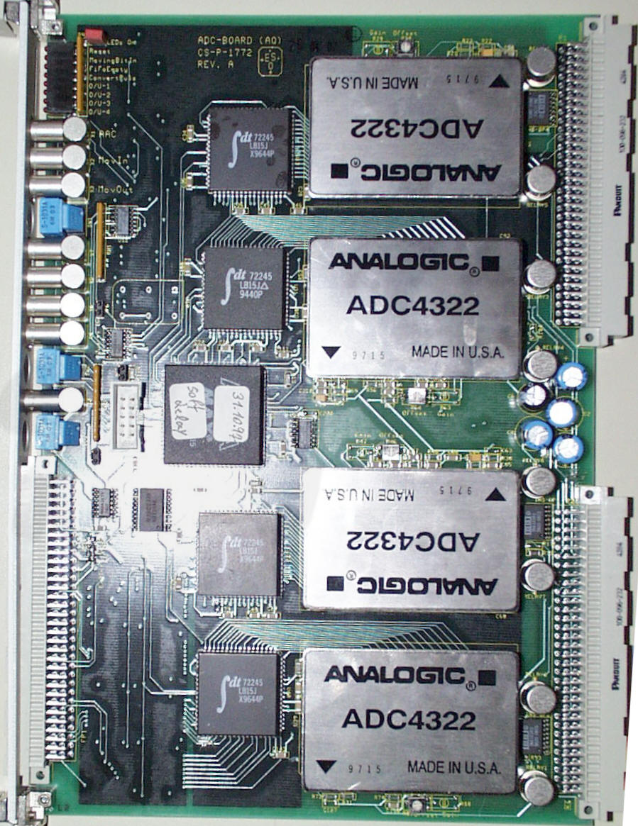 |
General DescriptionThe differential analogue input signals of each channel are input to an instrumentation amplifier followed by a low pass filters in front of the ADCs. A conversion command triggers the ADCs, the data are immediately transferred to a FIFO and then to the output registers. The convert signal has a programmable delay from 0 to 3 usec in steps of 200 nsec. Each acquisition module can be selected as a master module if the jumper number 8 is not set. It then generates a header code, corresponding to the header, which is set in the status register. Header word followed by the ADC data will put out over the GIGA bus. If the module is not a master, it just puts out the ADC data to the synchronous GIGA bus. To be synchron to another AQ, there is a signal called "Moving bit". Each module sends his data if the "MovingBitIn" signal is low (low active), after them it generates for the next Aq module the signal "MovingBitOut" and so on... |
|
AQ four channel (CS-P-1772- revision B)Features |
|
|
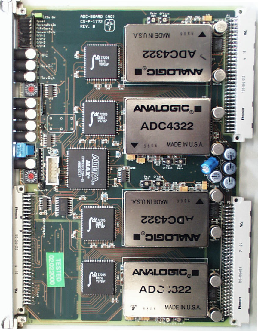 |
General DescriptionThe differential analogue input signals of each channel are input to an instrumentation amplifier followed by a low pass filters in front of the ADCs. A conversion command triggers the ADCs, the data are immediately transferred to a FIFO and then to the output registers. The convert signal has a programmable delay from 0 to 3 usec in steps of 200 nsec. Each acquisition module can be selected as a master module if the jumper number 8 is not set. It then generates a header code, corresponding to the header, which is set in the status register. Header word followed by the ADC data will put out over the GIGA bus. If the module is not a master, it just puts out the ADC data to the synchronous GIGA bus. To be synchron to another AQ, there is a signal called "Moving bit". Each module sends his data if the "MovingBitIn" signal is low (low active), after them it generates for the next Aq module the signal "MovingBitOut" and so on... |
|
![]()
AQ four channel (CS-P-1921- revision B)Features |
|
|
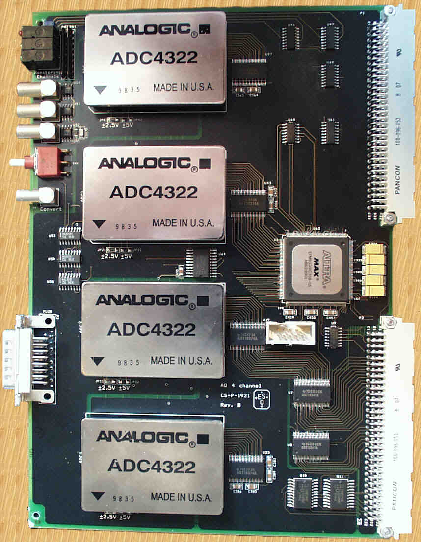 |
General DescriptionEach acquisition module will be selected automatically as a master module by the slot-ID (if it is set). It then generates a header code, corresponding to the header, which is set in the status register one. Header word followed by the ADC data will put out over the GIGA bus. If the module is not a master, it just puts out the ADC data to the synchronous GIGA bus. To be synchron to another AQ, there is a signal called "Moving bit". Each module sends his data if the "MovingBitIn" signal is low (low active), after them it generates for the next Aq module the signal "MovingBitOut" and so on... The acquisition module has sixteen channels and contains minimum digital logic, so those low-level analog signals are not disturbed by digital noise. The differential analog input signals of each channel are input to a discrete buildup amplifier followed by a low pass filters in front of the ADCs. A conversion command triggers the ADCs. The data are immediately transferred to the output registers. The convert signal has a programmable delay from 750 nsec (offset value) to 3 sec in steps of 50 nsec.. A conversion command triggers the ADCs, which has a convert time of 3 usec and the data are immediately transferred to the output registers. Each two output register (16 bit) send their data at the same time to the GIGA bus (32 bit width) on the P2 connector of backplane. The convert signal has a programmable delay from 0 to 3 sec in steps of 200 nsec. |
|
![]()
AQ 4-channel releases |
|||
| CS-P-1772- revision A | CS-P-1772- revision B | CS-P-1921- revision B | |
| Voltage range scalable | +/- 2.5 and +/- 5 | +/- 2.5 and +/- 5 | +/- 2.5 and +/- 5 |
| Number of different filters | 4 | 4 | 4 |
| Delay step of convert signal (ns) | 200 | 50 | 50 |
| Status bus-Id and header adjusable by | On board jumper | On board jumper | On back plane |
| Monitoring of ADC-inputs | Only difference signal | Only difference signal | signal plus/minus- and diff. |
| VME compatibility | Only P1 conn. | Only P1 conn. | P1 and P2 conn. |
| On board ADC-emulator | - | - | software controlled |
| Analog input signals entry | P2 conn. back panel | P2 conn. back panel | DSUB-25 front panel |
| ADC-Data output | P3 conn. front panel, flat-band cable | P3 conn. front panel, flat-band cable | P2 conn. back panel |
| FIFO buffered | implemented | implemented | - |
| Cascadable | over front panel lemo | over front panel lemo | over back panel |
![]()
|
|
|||