|
|
UVES Scientific CCD System |
||||
|
|
|
UVES Scientific CCD System |
||||
|
The mosaicing tolerances for the red mosaic assume that independent calibration will be performed for the two segments and that the spectra will be merged only after full data reduction.
| Item | Requirements | Obtained Results |
| Optical field size | 30.7 x 30.7 mm | 30.7 x 30.7 mm |
| BFD = The distance of the average CCD surface to the reference flange (mounting surface of field lens). |
4 mm + 0.25 - 0 | - |
| Centering = The distance between the optical center of the chip (not taking into accountpossible overscan pixels) and the mechanical axis of the dewar. |
< 0.5 mm | - |
| P-V flatness = The distance of the two planes, parallel to the reference flange, between which the sensitive surface of the chip or mosaic is contained. Applies to optical field size only. |
< 35 microns | 15 microns (room temperature) |
| Gap = Width of optically inactive area between two chips of the mosaic. The gap runs parallel to the readout direction but in case of bad CTE, we have the option of rotating the detector by 90°. One full order is lost in the gap. |
N. A. | N. A. |
| Pixel alignment = Conformity of the real position of any pixel compared to a perfect global pixel raster. If necessary for automatic line identification, the misalignments may be mapped (determination of Dx, Dy, j). The mapping is stable with time to a fraction of a pixel. |
N. A. | N. A. |
| Item | Requirements | Obtained Results |
| Optical field size | 61.4 x 61.4 mm | 61.4 x 61.4 mm |
| BFD = The distance of the average CCD surface to the reference flange (mounting surface of field lens). |
4 mm + 0.25 - 0 | - |
| Centering = The distance between the optical center of the chip (not taking into accountpossible overscan pixels) and the mechanical axis of the dewar. |
< 0.5 mm | - |
| P-V flatness = The distance of the two planes, parallel to the reference flange, between which the sensitive surface of the chip or mosaic is contained. Applies to optical field size only. |
< 50 (25) microns | 62 microns (cold) |
| Gap = Width of optically inactive area between two chips of the mosaic. The gap runs parallel to the readout direction but in case of bad CTE, we have the option of rotating the detector by 90°. One full order is lost in the gap. |
< 1000 (800) microns | 0.96 mm |
| Pixel alignment = Conformity of the real position of any pixel compared to a perfect global pixel raster. If necessary for automatic line identification, the misalignments may be mapped (determination of Dx, Dy, j). The mapping is stable with time to a fraction of a pixel. |
< 150 (30) microns | - |
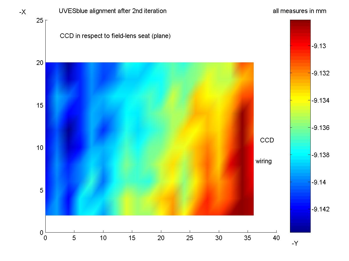
| Required value: | 9.125 ± 0.125 mm (at room temperature) |
| Obtained value: | 9.136 mm |
| rms | pv | |
| Analysis of the window back side | 0.0021 | 0.0064 |
| Analysis of the chip | 0.0064 | 0.0251 |
| Chip relative to the best fit plane of the window | 0.0148 | 0.0626 |
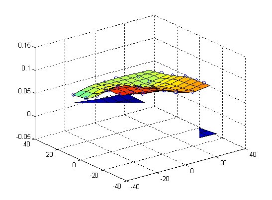
Topography of "NIGEL" and "STING" with respect to the window backside
at - 120 °C
|
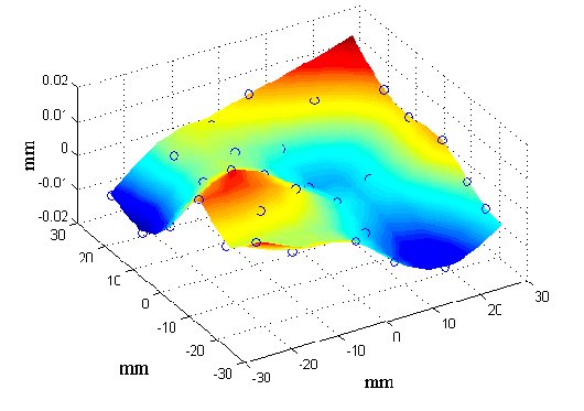
Topography of "NIGEL" and "STING" at - 120 °C
|
| Send comments to
<odt@eso.org>
Last update: Jan 27, 2010 Webdesign by EVI |
|