2 Standard Base Addresses and Interrupt Levels
This section lists standard addresses, interrupts etc. for the VLT standard boards.
2.1 Motorola MVME 167 CPU Board
Local address of on board memory: Standard VME (A24) 0 - 400 000 hex for a CPU with 4 MB ram
Extended VME (A32) 0 - 800 000 hex for a CPU with 8 MB ram
Extended VME (A32) 0 - 1 000 000 hex for a CPU with 16 MB ram
Extended VME (A32) 0 - 2 000 000 hex for a CPU with 32 MB ram
Only the RAM of the master CPU (processor 0) is accessible from the VMEbus. The memory is accessible in supervisory and non-privileged mode in program, data and block mode. The complete RAM is accessible. Bus snooping is enabled.
By default extended memory address 0 - 2 000 000 hex is cached. All other addresses are not cached.
On board memory of the master CPU is accessible from the VMEbus at the address:
Standard VME (A24) 800 000 hex for a CPU with 4 MB ram
Extended VME (A32) 1 000 000 hex for a CPU with 8 MB ram
Extended VME (A32) 2 000 000 hex for a CPU with 16MB ram
Extended VME (A32) 4 000 000 hex for a CPU with 32MB ram
Observe that Short I/O (A16) address space cc00 - cc0f hex is reserved by the CPU for mailbox interrupts.
Local base address (seen from the CPU) for VME address space:
Short I/O (A16) : 0xffff0000
Standard VME (A24) : 0xff000000
Extended VME (A32) : 0x00000000
The following interrupt vectors are reserved by VxWorks or the CPU:
Interrupt vectors reserved by VxWorks or the CPU
| Interrupt vector numbers (hex value) |
Usage |
| 00 - 0f |
MC680x0 exception vectors |
| 10 - 17 |
Unassigned |
| 18 - 1f |
Interrupt auto vectors |
| 20 - 2f |
Trap vectors |
| 30 - 37 |
Floating point processor(FPP) |
| 38 - 3f |
Memory management unit (MMU) |
| 40 - 5f |
CPU board UTIL1 |
| 60 - 6f |
CPU board UTIL2. These are not used |
| 90- -9f |
CPU board CD2400 (serial ports) |
More specifically VxWorks uses the following interrupt vectors:
Interrupt vectors used by VxWorks
| Interrupt vector number (hex value) |
Interrupt level |
Usage |
| 45 |
2 |
SCSI device |
| 46, 47 |
3 |
Ethernet |
| 48 |
5 |
Auxiliary clock |
| 49 |
6 |
System clock |
| 5e |
7 |
ABORT signal |
| 5f |
7 |
ACFAIL signal |
| 90- -9f |
4 |
Serial ports |
2.2 Motorola MVME 2604 CPU Board
Local address of on board memory:
Extended VME (A32) 0 - 1 000 000 hex for a CPU with 16 MB ram
Extended VME (A32) 0 - 2 000 000 hex for a CPU with 32 MB ram
Extended VME (A32) 0 - 4 000 000 hex for a CPU with 64 MB ram
Extended VME (A32) 0 -20 000 000 hex for a CPU with 512 MB ram
Only the RAM of the master CPU (processor 0) is accessible from the VMEbus.
Local base address (seen from the CPU) for VME address space:
Short I/O (A16) : 0xfbff0000
Standard VME (A24) : 0xfa000000
Extended VME (A32) : 0x10000000
2.3 TIM Board
| Base address (hex) |
Interrupt level |
Interrupt vector number (hex value) |
| Short I/O (A16) 100 |
6 |
80 |
2.4 ACRO 9481 Digital I/O Board
| Board |
Base address (hex) |
Interrupt level |
Interrupt vector number (hex value) |
| 0 |
Short I/O (A16) 1000 |
1 |
70 |
| 1 |
Short I/O (A16) 1400 |
1 |
71 |
| 2 |
Short I/O (A16) 1800 |
1 |
72 |
| 3 |
Short I/O (A16) 1c00 |
1 |
73 |
| 4 |
Short I/O (A16) 2000 |
1 |
74 |
| 5 |
Short I/O (A16) 2400 |
1 |
75 |
| 6 |
Short I/O (A16) 2800 |
1 |
76 |
| 7 |
Short I/O (A16) 2c00 |
1 |
77 |
2.5 VMIC VMIVME-3111 Analog I/O Board
| Board |
Base address (hex) |
Interrupt level |
Interrupt vector number (hex value) |
| 0 |
Short I/O (A16) 3000 |
1 |
78 |
| 1 |
Short I/O (A16) 3020 |
1 |
79 |
| 2 |
Short I/O (A16) 3040 |
1 |
7a |
| 3 |
Short I/O (A16) 3060 |
1 |
7b |
| 4 |
Short I/O (A16) 3080 |
1 |
7c |
| 5 |
Short I/O (A16) 30a0 |
1 |
7d |
| 6 |
Short I/O (A16) 30c0 |
1 |
7e |
| 7 |
Short I/O (A16) 30e0 |
1 |
7f |
2.6 MAC4 Motion Controller Board
| Board |
Base address (hex) |
Interrupt level |
Interrupt vector number (hex value) |
Backplane address |
| 0 |
Standard VME (A24) c10000 |
1 |
a0 - ae |
1 |
| 1 |
Standard VME (A24) c20000 |
1 |
b0 - be |
2 |
| 2 |
Standard VME (A24) c30000 |
1 |
c0 - ce |
3 |
| 3 |
Standard VME (A24) c40000 |
1 |
d0 - de |
4 |
| 4 |
Standard VME (A24) c50000 |
1 |
e0 - ee |
5 |
| 5 |
Standard VME (A24) c60000 |
1 |
f0 - fe |
6 |
2.7 VME4SA Servo Amplifier Board
| Board |
Base address (hex) |
Backplane address |
| 0 |
Short I/O (A16) 3100 |
1 |
| 1 |
Short I/O (A16) 3200 |
2 |
| 2 |
Short I/O (A16) 3300 |
3 |
| 3 |
Short I/O (A16) 3400 |
4 |
| 4 |
Short I/O (A16) 3500 |
5 |
| 5 |
Short I/O (A16) 3600 |
6 |
2.8 INMOS B016 Transputer Interface Board
| Board |
Base address (hex) |
Interrupt level |
Interrupt vector number (hex value) |
| 0 |
Short I/O (A16) 4000 Extended VME (A32) 2 000 000 |
3 |
|
1
The selection of interrupt vector conflicts with MAC4 board 2. B016 and 3 MAC4 can't be used in the same system.
|
2.9 ESD ISER8 8 (10) Channel Serial Interface Board
| Board |
Base address (hex) |
Interrupt level |
Interrupt vector number (hex value) |
| 0 |
Standard VME (A24) d00000 |
1 |
|
1
The selection of interrupt vector conflicts with MAC4 board 4 and 5. ISER8 can't be used in a system with more than 4 MAC4 controllers
|
2.10 Heidenhain IK 320 Encoder Interface Board
The following setting is valid for boards in one latch group. This is normally used when all boards are connected to the same encoder.
| Board |
Base address (hex) |
Interrupt level |
Interrupt vector number (hex value) |
| 0 |
Standard VME (A24) cfc000 Short I/O (A16) 8000 |
3 |
8f |
| 1 |
Standard VME (A24) cf8000 Short I/O (A16) 8000 |
3 |
8e |
| 2 |
Standard VME (A24) cf4000 Short I/O (A16) 8000 |
3 |
8d |
| 3 |
Standard VME (A24) cf0000 Short I/O (A16) 8000 |
3 |
8c |
| 4 |
Standard VME (A24) cec000 Short I/O (A16) 8000 |
3 |
8b |
| 5 |
Standard VME (A24) ce8000 Short I/O (A16) 8000 |
3 |
8a |
The following setting is valid for boards in different latch groups. This is normally used when all boards are connected to the different encoders.
| Board |
Base address (hex) |
Interrupt level |
Interrupt vector number (hex value) |
| 0 |
Standard VME (A24) cfc000 Short I/O (A16) 8000 |
3 |
8f |
| 1 |
Standard VME (A24) cf8000 Short I/O (A16) a000 |
3 |
af |
| 2 |
Standard VME (A24) cf4000 Short I/O (A16) c000 |
3 |
cf |
| 3 |
Standard VME (A24) cf00000 Short I/O (A16) e000 |
3 |
ef |
2.11 VMIC VMIVME - 5576 Reflective Memory Board
| Board |
Base address (hex) |
Interrupt level |
Interrupt vector number (hex value) |
| 0 |
Standard VME (A24) 000000 or extended VME (A32) 12000000 |
5 |
|
| 1 |
Standard VME (A24) 100000 or extended VME (A32) 12100000 |
5 |
|
1
The selection of interrupt vector conflicts with Acromag Digital I/O board 4,5,6 and 7. VMIVME - 5576 can't be used in a system with more than 4 Acromag Digital I/O boards.
2
The selection of interrupt vector conflicts with VMIC Analog I/O board 4,5,6 and 7. The second VMIVME - 5576 can't be used in a system with more than 4 VMIC Analog I/O boards.
|
2.12 NAT Net01 Ethernet Board
| Board |
Base address (hex) |
Interrupt level |
Interrupt vector number (hex value) |
| 0 |
Standard VME (A24) d00000 |
3 |
|
| 1 |
Standard VME (A24) d80000 |
3 |
c1 |
1
The selection of interrupt vector conflicts with MAC4 board # 3. Net01 can't be used in a system with more than 2 MAC4 controllers
|
3 Standard Jumper Setting
This section defines the jumper setting for the standard boards, in particular with the addresses and interrupt vectors defined in the previous section.
3.1 VMEbus Backplane
VMEbus Jumper must be installed between (if not automatic daisy chain)
for all empty VMEbus slots.
Jumper must be omitted between
for all VMEbus non-empty slots.
It is recommended also to install jumpers between
for all empty VMEbus slots.
3.2 Motorola MVME167 CPU Board
| Mandatory setting |
Jumper |
State |
Function |
|
|
J1 |
User defined |
General purpose readable jumper |
| M |
J2 |
Installed on master CPU (CPU 0). Omitted on all other CPUs on the same VMEbus |
System controller |
|
|
J6 |
User defined |
Serial port 4 receive clock configuration |
|
|
J7 |
User defined |
Serial port 4 transmit clock configuration |
| M |
J8 |
1 - 2 installed |
SRAM backup power from VMEbus +5 V STDBY |
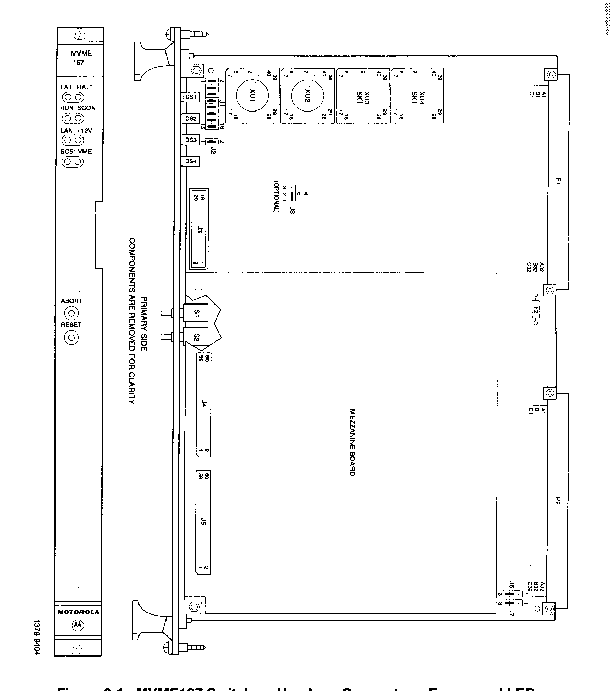
MVME 167 - jumper positions
3.3 Motorola MVME-2604 PowerPC CPU Board
| Mandatory setting |
Jumper |
State |
Function |
| M |
J3 |
Omitted |
Cache write-through always |
| M |
J10 |
1 - 2 installed |
Flash bank A enabled |
|
|
J16 |
User defined |
Serial port 4 receive clock |
|
|
J17 |
User defined |
Serial port 4 transmit clock |
|
|
J18 |
User defined |
Serial port 3 transmit clock |
|
|
J20 |
User defined |
Serial port 4 receive buffer |
|
|
J22 |
2 - 3 |
Auto system controller |
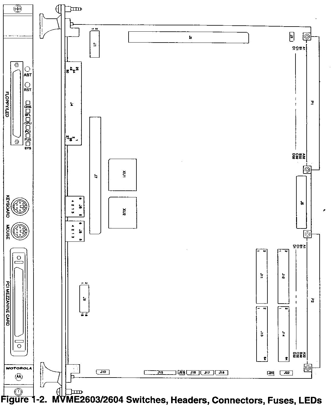
MVME 2604 - jumper locations
3.4 Motorola MVME 712M Transition Module
\
| Mandatory setting |
Jumper |
State |
Function |
| M |
J1, J11 |
J1 all installed J11 all omitted |
Serial port 1 configured as DCE (terminal) |
|
|
J16, J17 |
User defined |
Serial port 2 |
|
|
J13, J14 |
User defined |
Serial port 3 |
|
|
J18, J19 |
User defined |
Serial port 4 |
|
|
J15 |
User defined |
Serial port 4 clock |
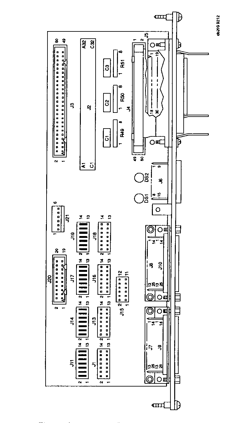
MVME 712M - jumper locations
3.5 TIM Board
| Mandatory setting |
Jumper |
State |
Function |
| M |
JP1 |
15 - 16 installed |
Base address setting ffff0100 hex |
| M |
JP2, JP3 |
JP2: 11 - 12 installed JP3: 3 - 4 and 5 - 6 installed |
Interrupt request level 6 |
|
|
JP4 |
1 - 2 installed |
Time bus signal source via the P2 connector |
|
|
JP5 |
Omitted |
No termination of time bus signal on the TIM board |
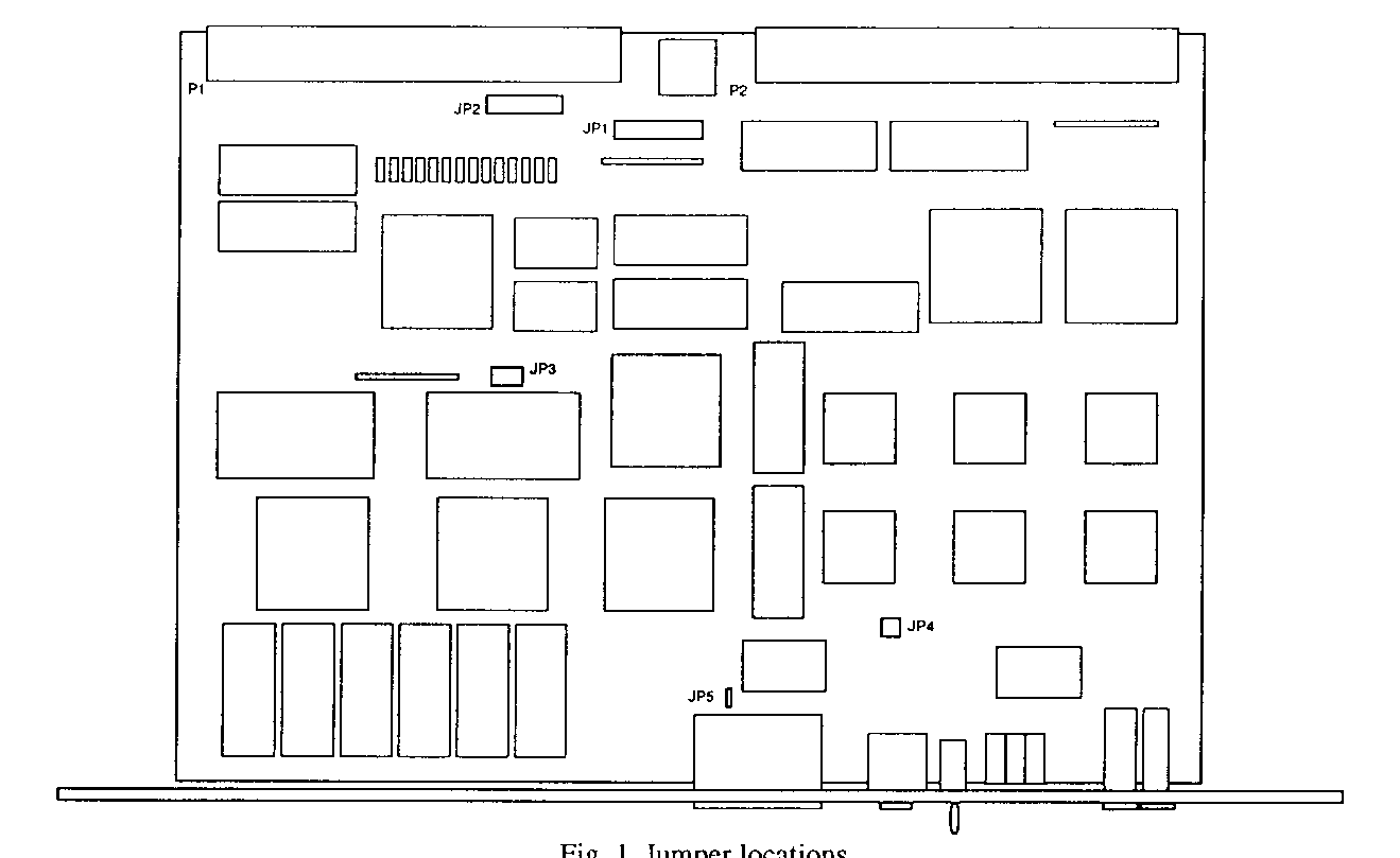
TIM - jumper locations
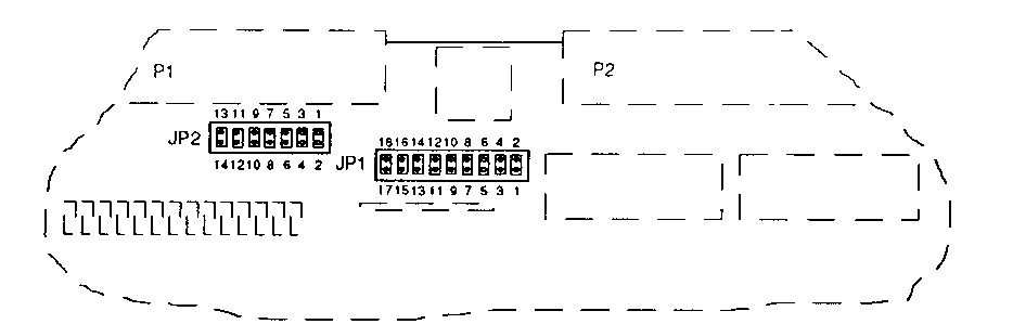
TIM - JP1 and JP2 jumper pin numbering
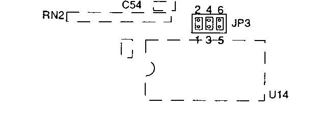
TIM - JP3 jumper pin numbering
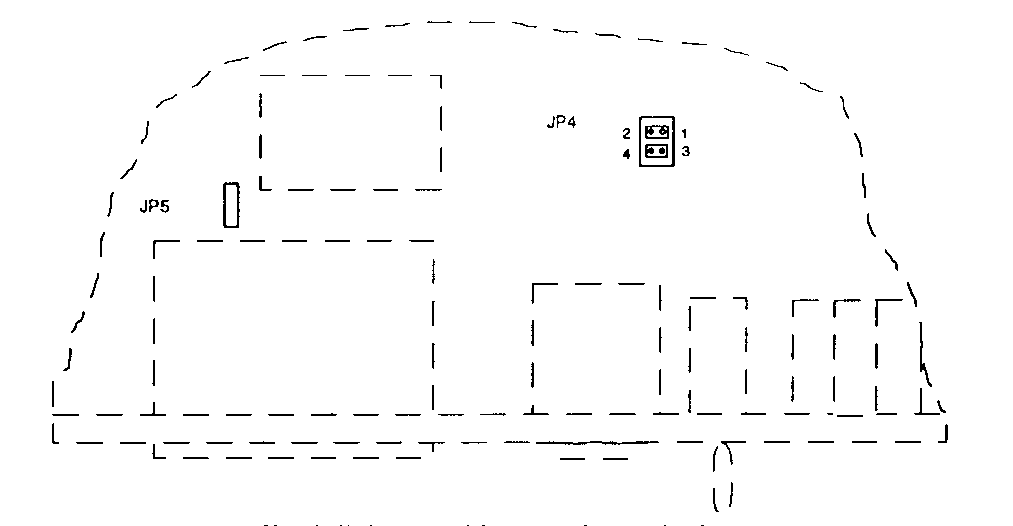
TIM - JP4 and JP5 jumper pin numbering
3.6 TIM Backplane Receiver
| Mandatory setting |
Jumper |
State |
Function |
|
|
JP1 |
1 - 2 and 5 - 6 installed |
Time Bus fiber connected on TIM backplane receiver, route to TIM P2 only. |
TIM backplane receiver - JP1 jumper pin numbering
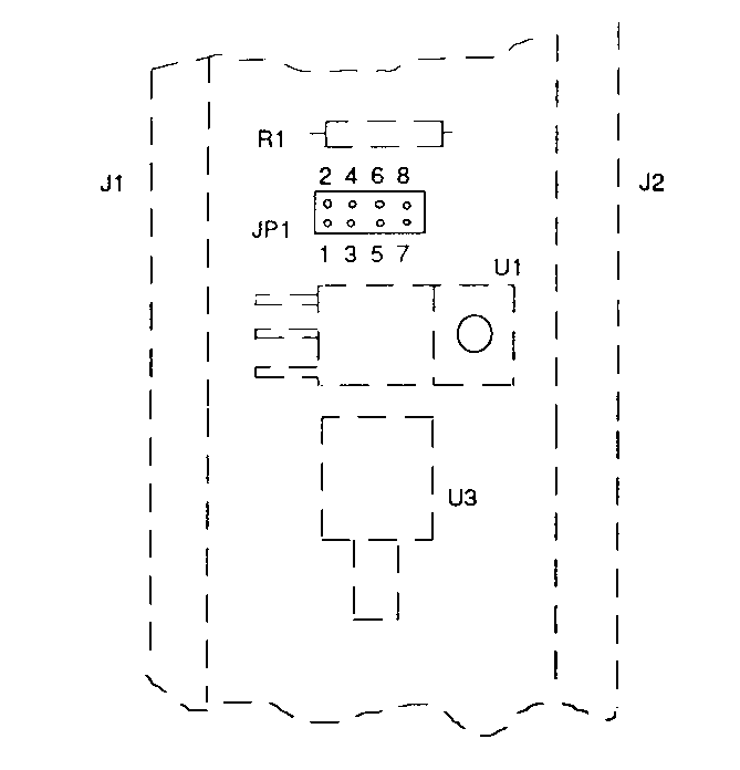
3.7 ACRO 9481 Digital I/O Board
| Mandatory setting |
Jumper |
State |
Function |
|
|
J1, J3, J5, J7 |
Installed |
Internal pullup to +5V of the I/O lines of port 4 and 5, 6 and 7, 2 and 3, 0 and 1 respectively |
|
|
J2, J4, J6, J8 |
Installed |
Internal threshold reference of the input lines of port 4 and 5, 6 and 7, 2 and 3, 0 and 1 respectively. |
| M |
J17 |
Base address: board 0: 5 - 6 installed board 1: 1 - 2, 5 - 6 installed board 2: 3 - 4, 5 - 6 installed board 3: 1 - 2, 3 - 4, 5 - 6 installed board 4: 7 - 8 installed board 5: 1 - 2, 7 - 8 installed board 6: 3 - 4, 7 - 8 installed board 7: 1 - 2, 3 - 4, 7 - 8 installed |
Base address: ffff1000 hex ffff1400 hex ffff1800 hex ffff1c00 hex ffff2000 hex ffff2400 hex ffff2800 hex ffff2c00 hex |
|
|
J19 |
Installed |
Short supervisory and non-privileged access |
|
|
J20 |
Omitted |
SYSFAIL is not asserted after reset |
Acromag 9481 - jumper locations
3.8 VMIC VMIVME-3111 Analog I/O Board
Default setting is:
Analog inputs: 16 differential, -10V to +10V range.
Analog outputs: single ended, -10V to +10V range.
| Mandatory setting |
Jumper |
State |
Function |
|
|
J1 |
Installed |
Ground P3 return |
|
|
J2 |
Installed |
Ground P3 sense |
| M |
J3 |
Omitted |
5 V full scale input not used |
| M |
J4 |
1 - 2 installed |
Bipolar analog inputs |
| M |
J5 |
2 - 3 installed |
Auto input gain adjust |
| M |
J6 |
Omitted |
Unipolar analog inputs not enabled |
| M |
J7, J8 |
Omitted |
Output test is validated |
|
|
J9, J10, J11 |
Omitted |
P3 inputs enabled |
| M |
J12 |
1 - 2 installed |
Bipolar analog outputs |
| M |
J13 |
Omitted |
20 V full scale output range |
| M |
J15 |
1 - 2 installed |
20 V full scale input range |
|
|
J17 - J24, J27 - J34 |
Omitted |
Differential input signals |
| M |
J25 |
Omitted |
2.5 VDC reference not used |
| M |
J26 |
Installed |
10 VDC reference used |
| M |
J35 |
Installed |
Ground P2 sense |
| M |
J36, J37 |
Base address: board 0: J36: 0, 1, 2, 3, 6, 7 installed J37: 0, 1, 2 installed board 1: J36: 0, 1, 2, 3, 6, 7 installed J37: 1, 2 installed board 2: J36: 0, 1, 2, 3, 6, 7 installed J37: 0, 2 installed board 3: J36: 0, 1, 2, 3, 6, 7 installed J37: 2 installed |
Base address: ffff3000 hex
ffff3020 hex
ffff3040 hex
ffff3060 hex |
| M |
J37-3 |
Omitted |
Short supervisory access |
| M |
J38 |
2 - 3 installed |
Auto input zero adjust |
| M |
J39 |
Installed |
Ground analog outputs return |
| M |
J40 |
Omitted |
5 VDC reference not used |
|
|
J41 |
Omitted |
External trigger not connected to P2 GND sense |
|
|
J42 |
1 - 2 installed |
External trigger RTN connected to P2 GND sense |
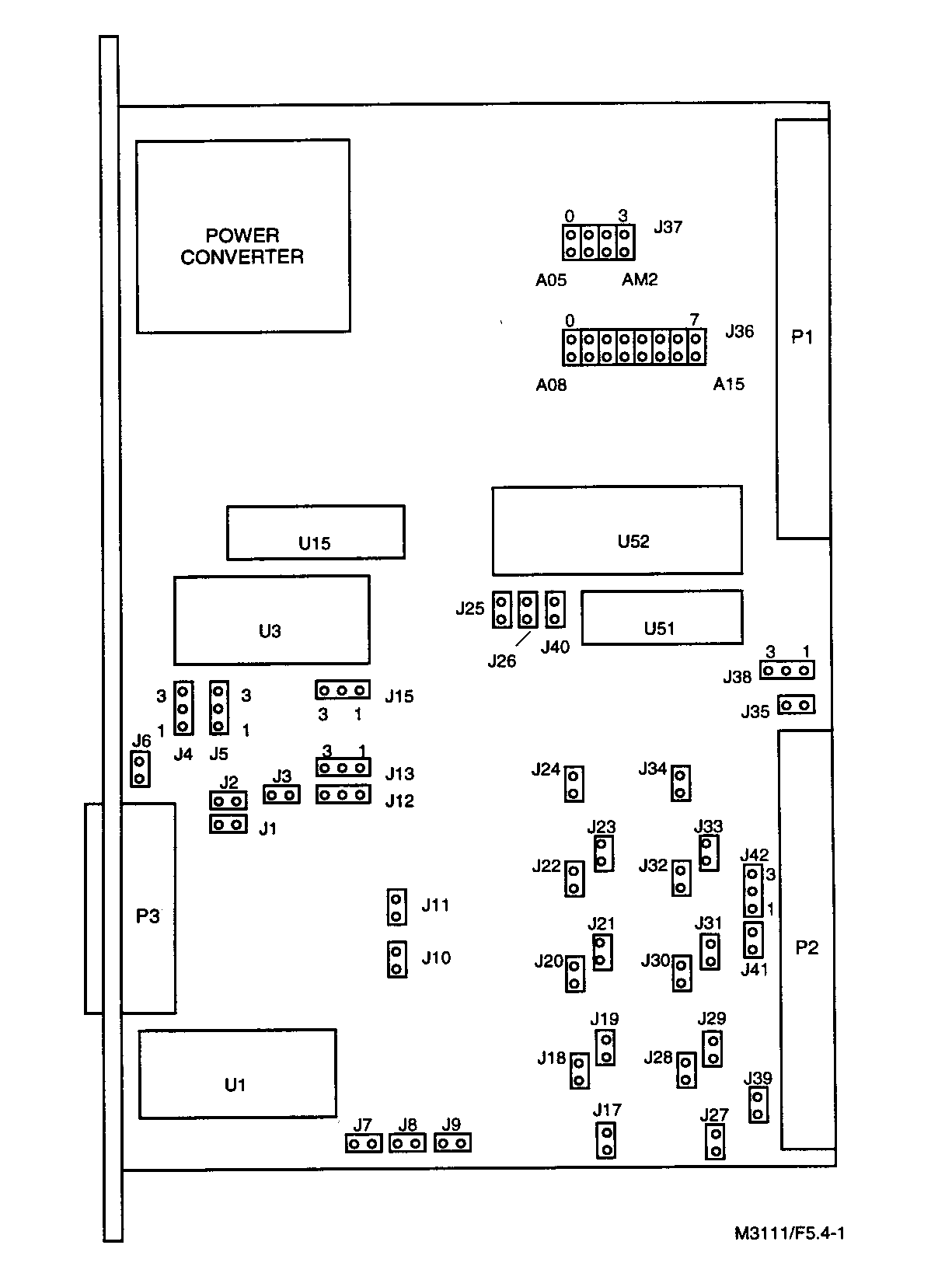
VMIVME 3111 - jumper locations
3.9 MAC 4 Motion Controller
| Mandatory setting |
Jumper |
State |
Function |
| M |
J3 |
Installed |
No system controller |
| M |
J4 |
AB installed |
Reset from push-button and VMEbus |
| M |
J7 |
AB installed |
Interrupt requests are not handled |
|
|
J8 |
Omitted |
Timer C output not connected with timer B input (internal use only) |
| M |
J11 |
Installed |
Watchdog on (internal watchdog used for reset) |
| M |
S1, S2 |
Base address: board 0: S1 = c, S2 = 1 board 1: S1 = c, S2 = 2 board 2: S1 = c, S2 = 3 board 3: S1 = c, S2 = 4 board 4: S1 = c, S2 = 5 board 5: S1 = c, S2 = 6 |
Base address: c10000 hex c20000 hex c30000 hex c40000 hex c50000 hex c60000 hex |
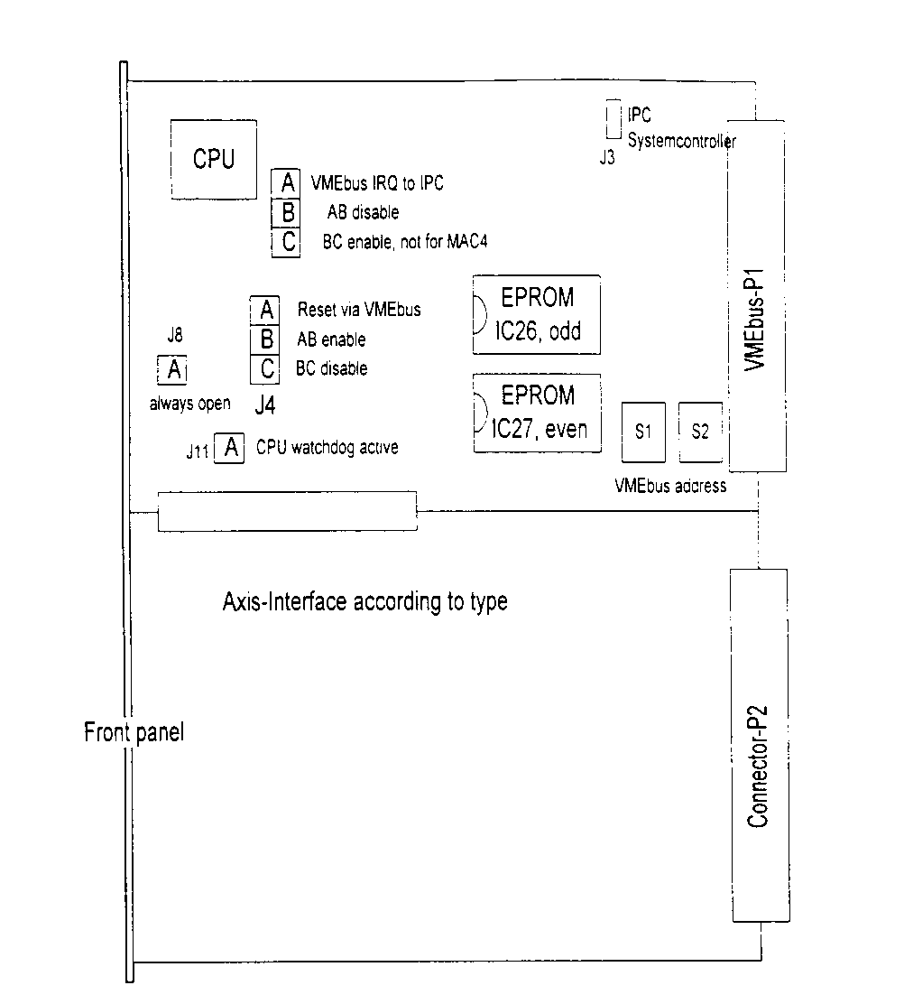
MAC4 IPC - jumper locations
3.10 MAC4 SSI IPC
| Mandatory setting |
Jumper |
State |
Function |
|
|
J1 |
Installed: binary code, omitted: gray code, A: axis 1 B: axis 2 C: axis 3 D: axis 4 |
Encoder data coding |
|
|
J2 |
A: 93.75 kHz B: 187.5 kHz C: 375 kHz D: 750 kHz |
Encoder clock rate |
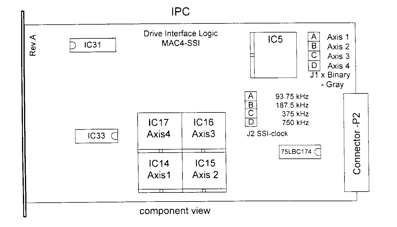
MAC4 SSI - jumper locations
3.11 VME4SA Servo Amplifier Board
| Mandatory setting |
Jumper |
State |
Function |
| M |
CN4 |
1 - 2 installed |
Wait mode for read-out |
| M |
SW1 |
Base address: board 0: 1, 2, 5, 6, 7 on 3, 4, 8 off board 1: 1, 2, 5, 6, 8 on 3, 4, 7 off board 2: 1, 2, 5, 6 on 3, 4, 7, 8 off board 3: 1, 2, 5, 7, 8 on 3, 4, 6 off board 4: 1, 2, 5, 7 on 3, 4, 6, 8 off board 5: 1, 2, 5, 8 off 3, 4, 6, 7 on |
Base address: ffff3100 hex
ffff3200 hex
ffff3300 hex
ffff3400 hex
ffff3500 hex
ffff3600 hex
|
VME4SA - jumper locations
3.12 VME4SA P2 Backplane
| Mandatory setting |
Jumper |
State |
Function |
| M |
BR1 |
Backplane address: backplane 0: 0 omitted 1, 2, 3 installed backplane 1: 1 omitted 0, 2, 3 installed backplane 2: 0, 1 omitted 2, 3 installed backplane 3: 2 omitted 0, 1, 3 installed backplane 4: 0, 2 omitted 1. 3 installed backplane 5: 1, 2 omitted 0, 3 installed |
Base address 1
2
3
4
5
6 |
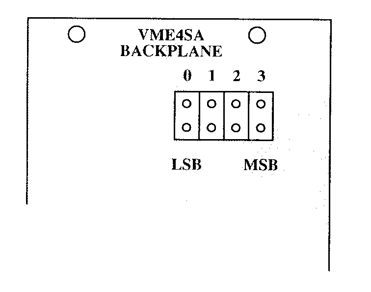
VME4SA Backplane - jumper positions
3.13 INMOS B016 Transputer Interface Board
| Mandatory setting |
Jumper |
State |
Function |
| M |
SW2, SW3 |
Base address: SW2: 4, SW3: 0 |
Base address ffff4000 (A16) hex |
| M |
K1 |
Omitted |
IMS T801 boots from F-ROM |
| M |
K2 |
Omitted |
IMS T801 links are 20 MBits/s |
| M |
K3 |
Omitted |
No VMEbus master |
| M |
K4 |
Omitted |
No F-ROM programming |
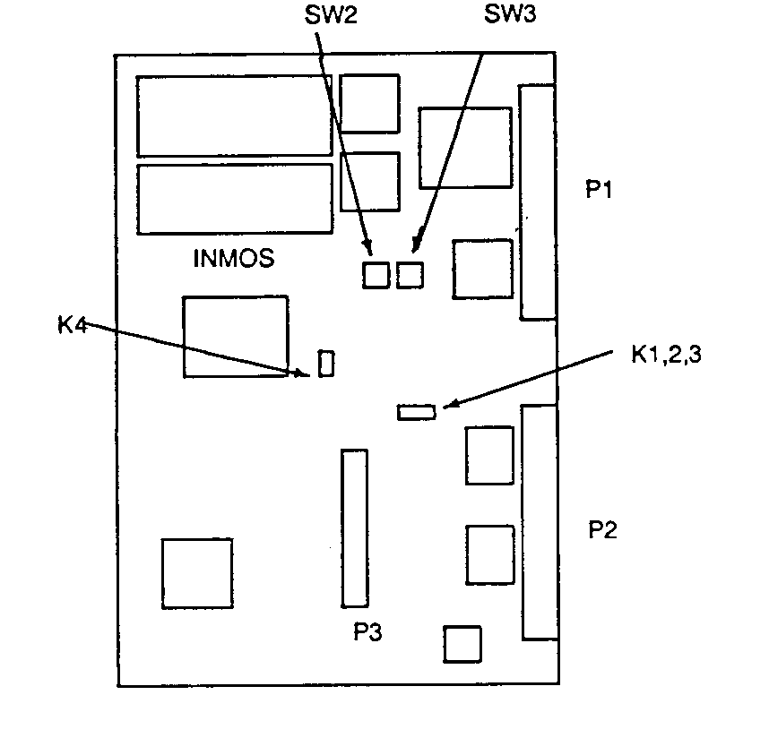
B016 - jumper locations
3.14 ESD ISER8 8 (10) Channel Serial Interface Board
| Mandatory setting |
Jumper |
State |
Function |
| M |
J1 |
7 - 9 installed |
Standard supervisory and non-privileged data access |
| M |
J2, J7, J8 |
Base address: J2: 5 - 6 installed J7, J8 omitted |
Base address d00000 hex |
|
|
J3 |
2 - 4 installed |
No synchronous mode of channel 9 |
|
|
J3A |
2 - 4 installed |
No synchronous mode of channel 10 |
|
|
J4 |
3 - 4 installed |
DTACK delay of 140 ns |
|
|
J6, J9 |
2 - 3 installed |
+5V supply of the piggy-backs |
|
|
J11 |
Omitted |
Memory size 128 kB RAM, 128 kB EPROM |
|
|
J12 |
User defined |
General purpose readable jumper |
|
|
J13, J14 |
Omitted |
Asynchronous mode of channel 10 |
|
|
J16 |
Omitted |
Watchdog 1.2 seconds |
| M |
J17 |
Omitted |
No VMEbus RESET generated |
|
|
J26 |
Omitted |
Asynchronous mode of channel 9 |
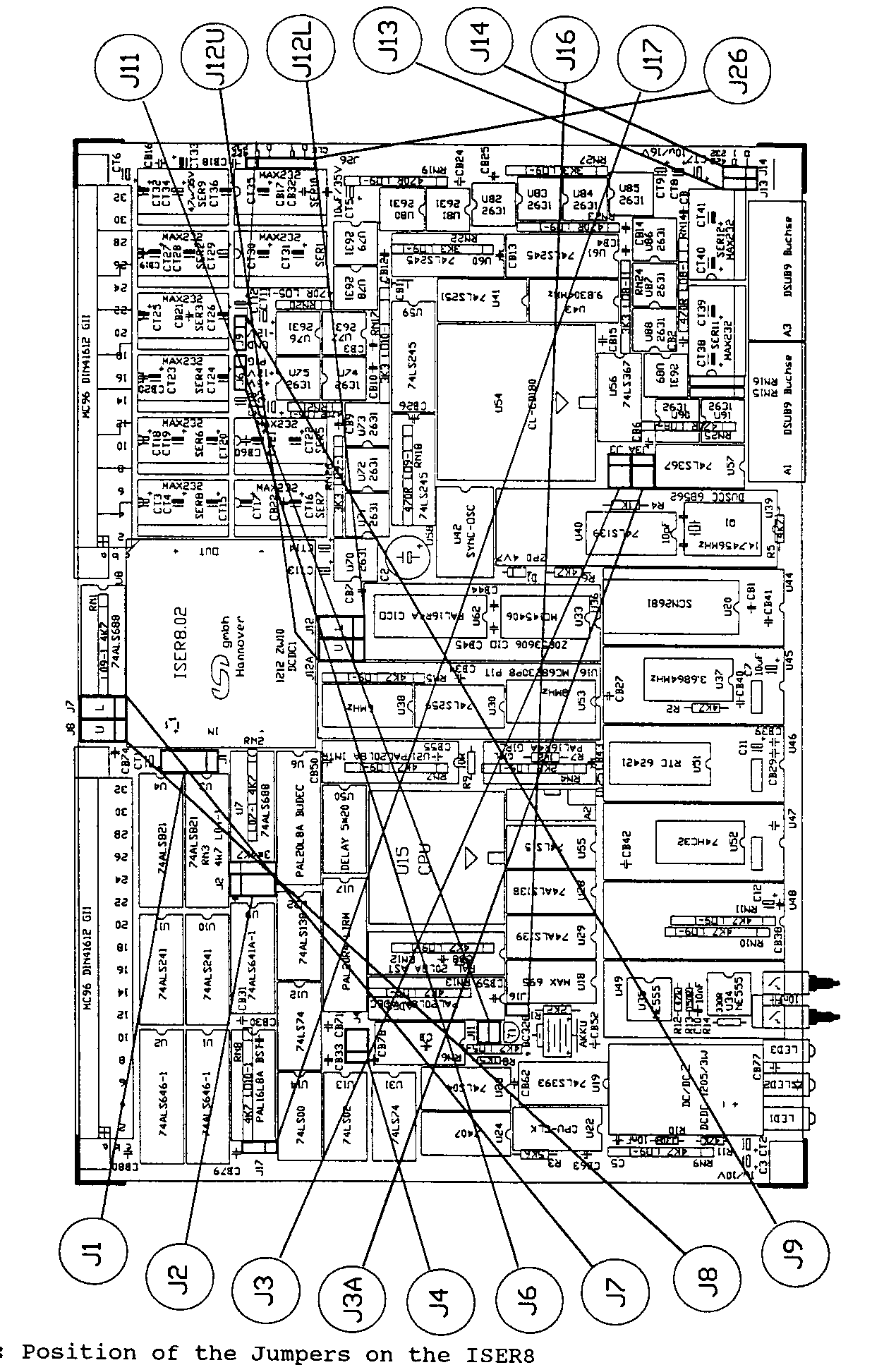
ISER8 - jumper locations
3.15 Heidenhain IK 320 Encoder Interface Board
Jumper setting with all boards in one latch group
| Mandatory setting |
Jumper |
State |
Function |
| M |
SI, SII |
Base address and interrupt vector: board 0:SI: S5 - S7 ON S1 - S4, S8 OFF SII:S7 - S8 ON S1 - S6 OFF board 1: SI: S1, S5 - S7 ON S2 - S4, S8 OFF SII: S1, S7 - S8 ON S2 - S6 OFF Board 2: SI: S2, S5 - S7 ON S1, S3 - S4, S8 OFF SII: S2, S7 - S8 ON S1, S3 - S6 OFF board 3: SI: S1- S2, S5 - S7 ON S3 - S4, S8 OFF SII: S1 - S2, S7 - S8 ON S3 - S6 OFF board 4: SI: S3, S5 - S7 ON S1 - S2, S4, S8 OFF SII: S3, S7 - S8 ON S1 - S2, S4 - S6 OFF board 5: SI: S1, S3, S5 - S7 ON S2, S4, S8 OFF SII: S1, S3, S7 - S8 ON S2, S4 - S6 OFF |
Base address: ffff8000 (A16) Interrupt vector 8f cfc000 (A24)
ffff8000 (A16) Interrupt vector 8e cf8000 (A24)
ffff8000 (A16) Interrupt vector 8d cf4000 (A24)
ffff8000 (A16) Interrupt vector 8c cf0000 (A24)
ffff8000 (A16) Interrupt vector 8b cec000 (A24)
ffff8000 (A16) Interrupt vector 8a ce8000 (A24) |
| M |
J1 |
3 installed 1 - 2, 4 - 7 omitted |
Interrupt level 3 |
| M |
J2 |
3 installed 1 - 2, 4 - 7 omitted |
Interrupt level 3 |
| M |
J3 |
Board 0: installed board 2 - 5: omitted |
DTACK on address cycle No DTACK on address cycle |
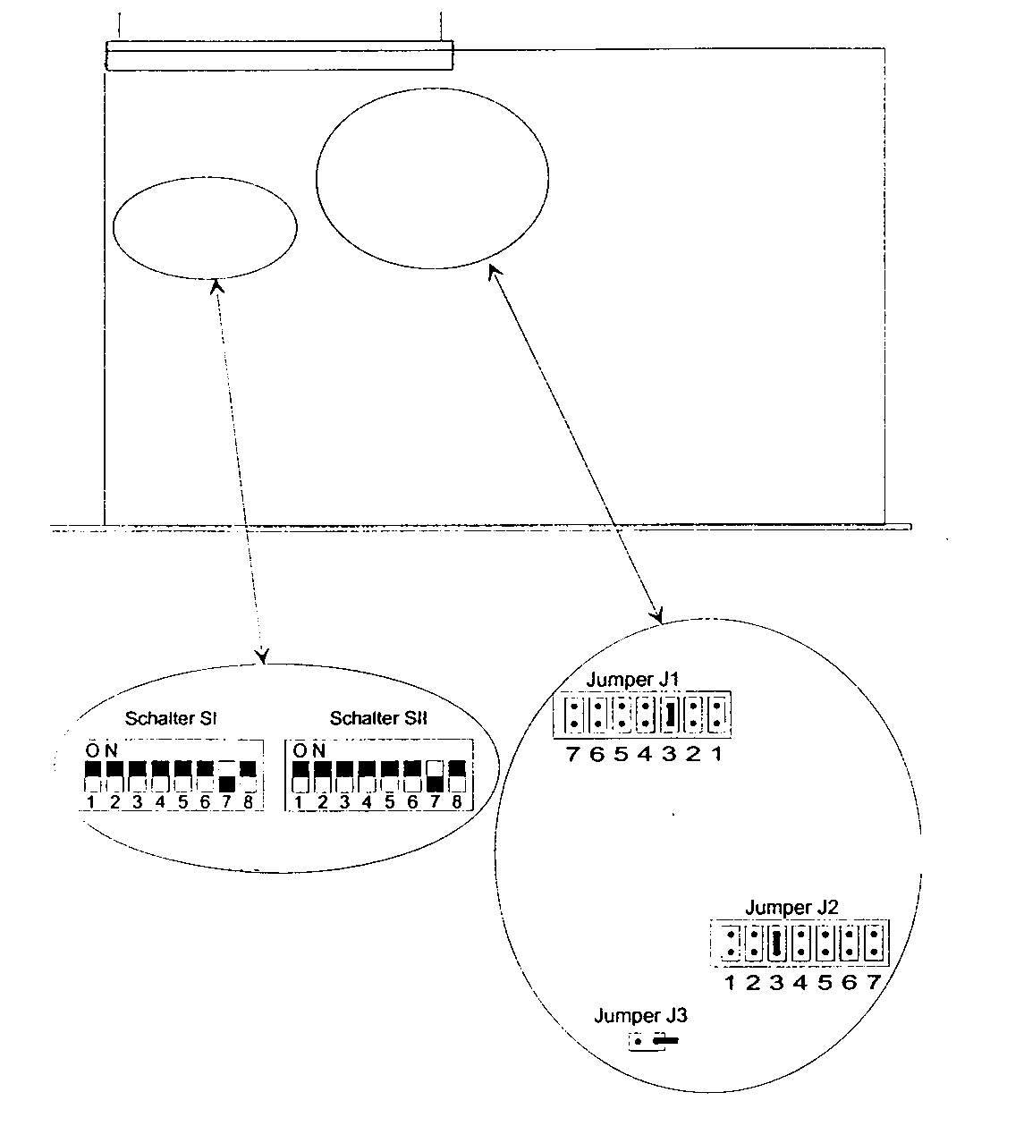
IK320 - jumper locations
Jumper setting with all boards in different latch groups
| Mandatory setting |
Jumper |
State |
Function |
| M |
SI, SII |
Base address and interrupt vector: board 0:SI: S5 - S7 ON S1 - S4, S8 OFF SII:S7 - S8 ON S1 - S6 OFF board 1: SI: S5, S7 ON S1 - S4, S6, S8 OFF SII: S1, S7 - S8 ON S2 - S6 OFF Board 2: SI: S5 - S6 ON S1 - S4, S7 - S8 OFF SII: S2, S7 - S8 ON S1, S3 - S6 OFF board 3: SI: S5 ON S1 - S4, S6 - S8 OFF SII: S1 - S2, S7 - S8 ON S3 - S6 OFF |
Base address: ffff8000 (A16) Interrupt vector 8f cfc000 (A24)
ffffa000 (A16) Interrupt vector af cf8000 (A24)
ffffc000 (A16) Interrupt vector cf cf4000 (A24)
ffffe000 (A16) Interrupt vector ef cf0000 (A24) |
| M |
J1 |
3 installed 1 - 2, 4 - 7 omitted |
Interrupt level 3 |
| M |
J2 |
3 installed 1 - 2, 4 - 7 omitted |
Interrupt level 3 |
| M |
J3 |
installed |
DTACK on address cycle |
3.16 VMIC VMIVME - 5576 Reflective Memory Board
| Mandatory setting |
Jumper |
State |
Function |
|
|
J1, J2 |
Default factory setting |
Installed memory option |
|
|
A1, A2, A3 |
Default factory setting |
|
| M |
J3 |
Installed |
INT0 is enabled |
| M |
J5 |
Omitted |
Data link rate is 6.2 MB/s |
|
|
J6 |
Omitted |
Not used |
| M |
J8 |
2 - 3 installed |
Both supervisory and non-privileged addressing |
|
|
J9 |
User defined |
Board node ID. Defines the node address in the reflective memory network. Each node must have a different node ID [0..255], installed jumper sets the corresponding bit to 0 |
|
|
J10 |
Installed |
Address Mode. Installed means A32 addressing, omitted A24 addressing. For automatic recognition at boot time, this choice must conform to the choice made in rmn.boot |
|
|
J4 |
Must be set to 0x12 if J10 is installed (convention :/0 = empty/installed) 000:00:0 |
Address A31 - A24 = 0x12000000 |
| M |
J7 |
Board address and memory option (convention :/0 = empty/installed) board): 00 0000 00 0: 0000 0: :: 0000 :: board1: 00 000: 00 0: 000: 0: :: 000: :: |
Base address 0x000000 (A24) or 0x12000000 (A32)
256 kB memory 512 kB memory 1 MB memory
256 kB memory 512 kB memory 1 MB memory |
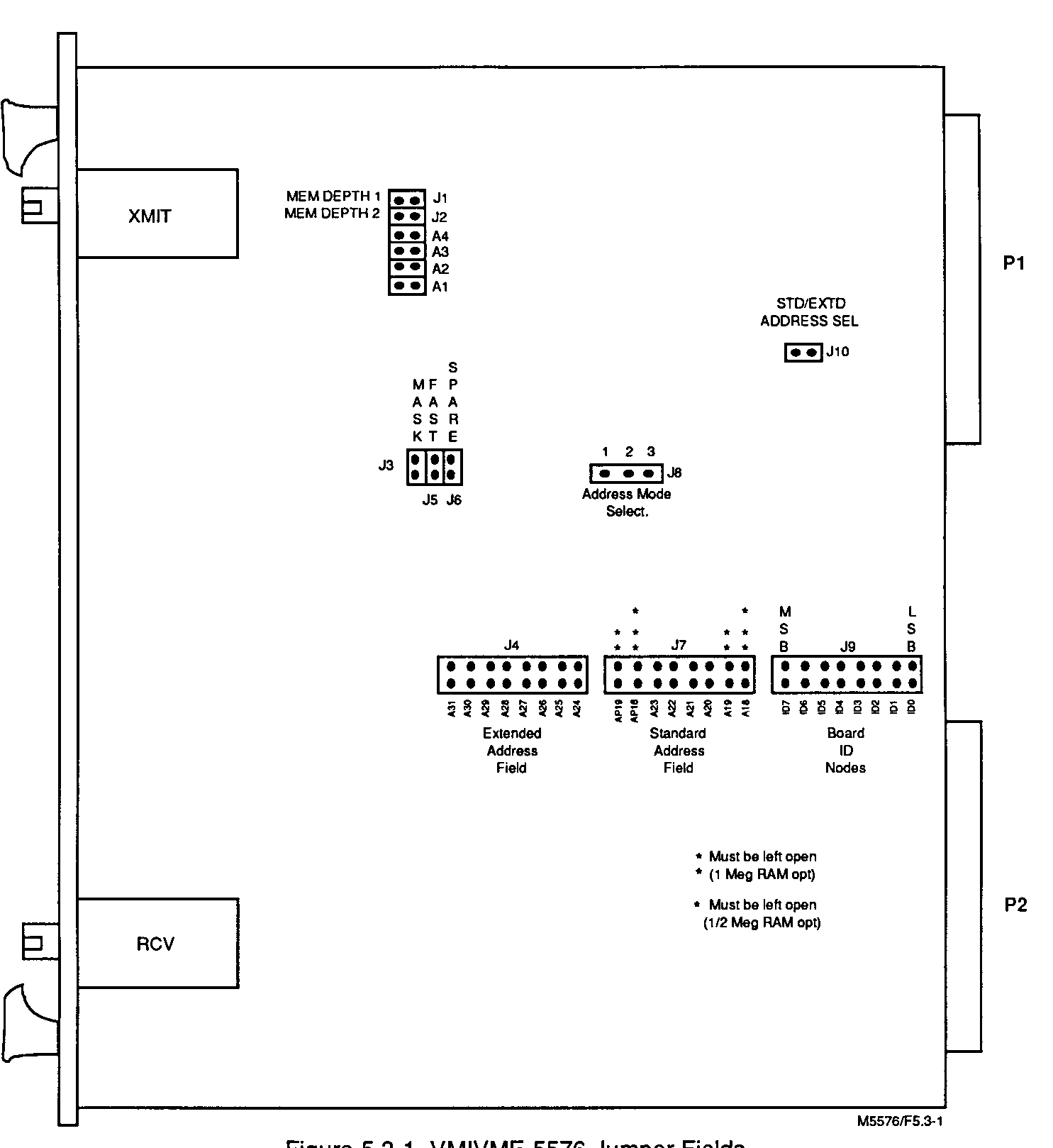
VMIVME 5576 - jumper locations
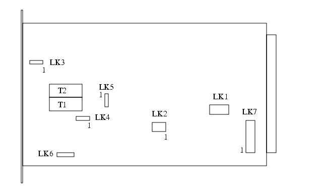
3.17 NAT Net01 Ethernet Board
| Mandatory setting |
Jumper |
State |
Function |
| M |
LK1 |
Base address (convention :/0 = empty/installed) board 0: ::0:0 board 1: ::0:: |
Base address:
d00000 hex d80000 hex |
| M |
LK2 |
1 and 3 installed, 2 omitted |
Interrupt level 3 |
| M |
LK7 |
3 installed |
Interrupt level 3 |
| M |
LK3 |
2 - 3 installed |
Grounding to system 0 V |
|
|
LK4 |
2 -3 installed |
SQE test enabled |
| M |
LK5 |
2 - 3 installed |
Idle output high |
| M |
LK6 |
Middle installed |
Transmit collision detection |
| M |
T1/2 |
T2 set (upper) |
AIU transceiver (T1 means BNC connection) |