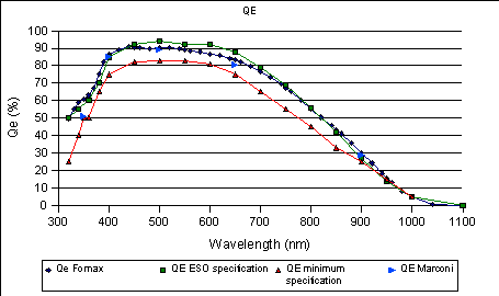
Figure 1: Comparison between the QE measured by ESO, the QE measured by Marconi, ESO specification and minimum specification.
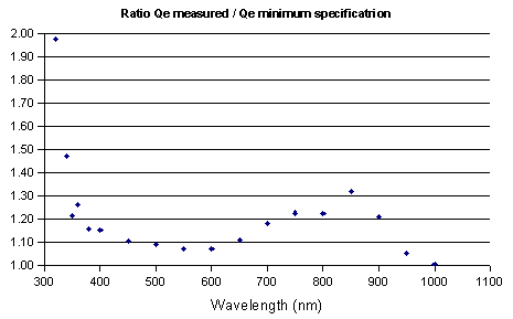
Figure 2: Ratio between the ESO measurements and the ESO minimum specification.
Measurement made by the: 27 June 2001 – 11 July 2001
Data
reduced by Fabrice Christen the: October 31st, 2001
Measure realized at -120 deg.
|
Wav. |
Qe Fornax |
Error |
PRNU RMS (%) |
Phase |
|
320 |
49.4 |
1.4 |
3.47 |
7.41 |
|
330 |
55.1 |
1.6 |
3.25 |
7.34 |
|
340 |
58.8 |
1.1 |
3.16 |
7.31 |
|
350 |
60.6 |
0.59 |
3.16 |
7.31 |
|
360 |
63.1 |
0.62 |
3.14 |
7.31 |
|
370 |
67.3 |
0.66 |
2.85 |
7.21 |
|
380 |
75.1 |
0.74 |
2.19 |
6.94 |
|
390 |
82.3 |
0.85 |
1.79 |
6.73 |
|
400 |
86.3 |
0.87 |
1.59 |
6.61 |
|
420 |
89.3 |
0.9 |
1.43 |
6.5 |
|
440 |
90.7 |
0.91 |
1.38 |
6.46 |
|
450 |
90.45 |
0.91 |
0 |
6.45 |
|
460 |
90.2 |
0.91 |
1.36 |
6.44 |
|
480 |
89.8 |
0.9 |
1.35 |
6.43 |
|
500 |
90.3 |
0.91 |
1.34 |
6.43 |
|
520 |
90.3 |
0.91 |
1.33 |
6.43 |
|
540 |
89.6 |
0.9 |
1.34 |
6.43 |
|
550 |
89 |
0.89 |
0 |
6.44 |
|
560 |
88.4 |
0.88 |
1.34 |
6.44 |
|
580 |
88.1 |
0.88 |
1.36 |
6.45 |
|
600 |
86.8 |
0.86 |
1.38 |
6.47 |
|
620 |
85.7 |
0.84 |
1.41 |
6.5 |
|
640 |
84.3 |
0.82 |
1.45 |
6.53 |
|
650 |
83.2 |
0.81 |
0 |
6.54 |
|
660 |
82.1 |
0.8 |
1.49 |
6.56 |
|
680 |
79.9 |
0.76 |
1.52 |
6.58 |
|
700 |
76.6 |
0.72 |
1.64 |
6.66 |
|
720 |
73.4 |
0.67 |
1.86 |
6.79 |
|
740 |
69.7 |
0.63 |
1.94 |
6.83 |
|
750 |
67.35 |
0.61 |
0 |
6.88 |
|
760 |
65 |
0.58 |
2.15 |
6.93 |
|
780 |
60.3 |
0.53 |
2.15 |
6.93 |
|
800 |
55.1 |
0.48 |
2.2 |
6.96 |
|
820 |
50.5 |
0.43 |
2.16 |
6.94 |
|
840 |
45.9 |
0.39 |
2 |
6.85 |
|
850 |
43.5 |
0.37 |
0 |
6.92 |
|
860 |
41.1 |
0.34 |
2.27 |
6.99 |
|
880 |
35.9 |
0.29 |
2.63 |
7.13 |
|
900 |
30.2 |
0.24 |
3.24 |
7.34 |
|
920 |
24.2 |
0.19 |
4.9 |
7.74 |
|
940 |
18.5 |
0.14 |
6.2 |
7.92 |
|
950 |
15.75 |
0.12 |
0 |
8.01 |
|
960 |
13 |
0.1 |
7.48 |
8.11 |
|
980 |
8.36 |
0.06 |
8.88 |
8.29 |
|
1000 |
5.01 |
0.04 |
9.92 |
8.35 |
|
1040 |
0.92 |
0.01 |
9.02 |
8.29 |
|
1100 |
0.13 |
0 |
8.98 |
8.35 |
Table 1: Measurement of the Quantum Efficiency.
In this section you can compare the QE we measured with the testbench and:
QE Minimum specification
Typical QE
QE from Marconi
|
|
|
|---|---|
Figure 1: Comparison between the QE measured by ESO, the QE measured by Marconi, ESO specification and minimum specification. |
Figure 2: Ratio between the ESO measurements and the ESO minimum specification. |
|
Special specification |
|||
|
Wavelength(nm) |
Minimum spec. (%) |
ESO measurements (%) |
Result |
|
350 |
50 |
60.6 |
OK |
|
400 |
80 |
86.3 |
OK |
|
650 |
80 |
83.2 |
OK |
|
900 |
25 |
30.2 |
OK |
|
Conclusion: |
Ok, this CCD is in the 25 % |
||
Table 2: Minimum specification for 25 % of the CCDs.
|
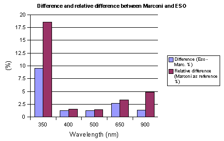
Comparison QE ESO and QE Marconi |
|||||
|
Wavelength (nm) |
QE ESO (%) |
Qe Marconi (%) |
Difference (Eso - Marc. %) |
Relative difference (Marconi as reference %) |
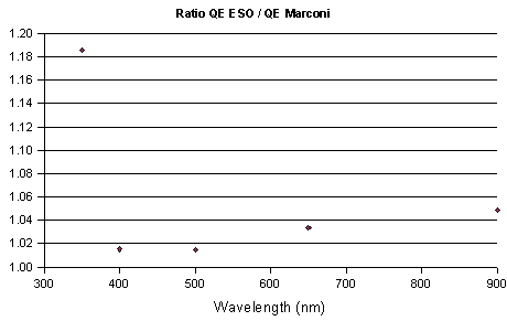
Ratio QE ESO / QE Marconi |
|
350 |
60.6 |
51.1 |
9.5 |
18.6 |
1.19 |
|
400 |
86.3 |
85 |
1.3 |
1.5 |
1.02 |
|
500 |
90.3 |
89 |
1.3 |
1.5 |
1.01 |
|
650 |
83.2 |
80.5 |
2.7 |
3.4 |
1.03 |
|
900 |
30.2 |
28.8 |
1.4 |
4.9 |
1.05 |
Table 3: Difference and relative difference between ESO measurements and Marconi.
|
|
|
|---|---|
Figure 3: Graphic representation of the difference and the relative difference. |
Figure 4: Ratio between the ESO measurements and the Marconi measurements |
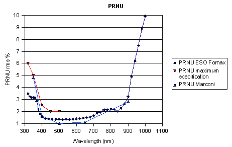
In this section you can compare the PRNU we measured at ESO and:
PRNU Minimum specification
PRNU from Marconi
|
|
|
|---|---|
|
Figure 5: Comparison between the PRNU measured by ESO, the PRNU measured by Marconi, and the maximum specification. |
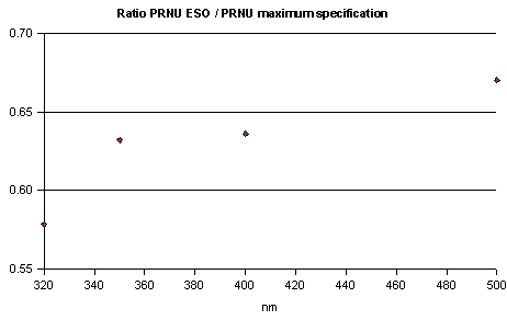
Figure 6: Ratio between the ESO measurements and the Maximum specification. |
|
|
|
|
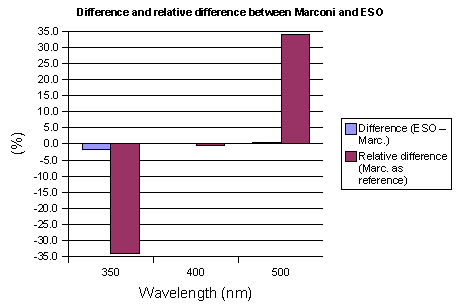
Figure 7: Graphic representation of the difference and the relative difference. |
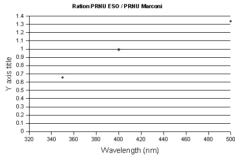
Figure 8: Ratio between the ESO measurements and the Marconi measurements. |
|
Comparison QE ESO and QE Marconi |
||||||
|
Wavelength (nm) |
PRNU ESO (rms %) |
Maximum spec. |
PRNU Marconi |
Difference (ESO – Marc.) |
Relative difference (Marc. as reference) |
Ratio PRNU ESO / PRNU Marconi |
|
320 |
3.47 |
6 |
0 |
0 |
0 |
0 |
|
350 |
3.16 |
5 |
4.8 |
-1.64 |
-34.17 |
0.66 |
|
400 |
1.59 |
2.5 |
1.6 |
-0.01 |
-0.62 |
0.99 |
|
500 |
1.34 |
2 |
1 |
0.34 |
34 |
1.34 |
Table 4: Difference and relative difference between ESO measurements and Marconi.
In this section you will see the if the values we have measured for the QE and the PRNU are in accordance with the contract.
|
Wavelength (nm) |
Qe |
PRNU |
|
320 |
OK |
OK |
|
340 |
OK |
|
|
350 |
OK |
OK |
|
360 |
OK |
|
|
380 |
OK |
|
|
400 |
OK |
OK |
|
450 |
OK |
OK |
|
500 |
OK |
OK |
|
550 |
OK |
|
|
600 |
OK |
|
|
650 |
OK |
|
|
700 |
OK |
|
|
750 |
OK |
|
|
800 |
OK |
|
|
850 |
OK |
|
|
900 |
OK |
|
|
950 |
OK |
|
|
1000 |
OK |
|
Table 5: Comparison between the values we have measured and the specifications in the contract.
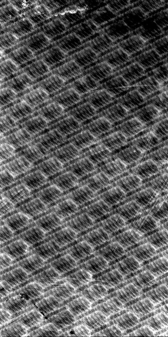
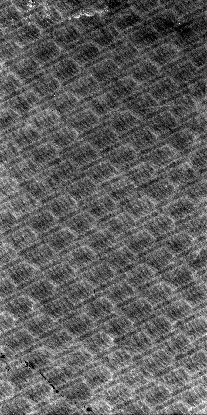
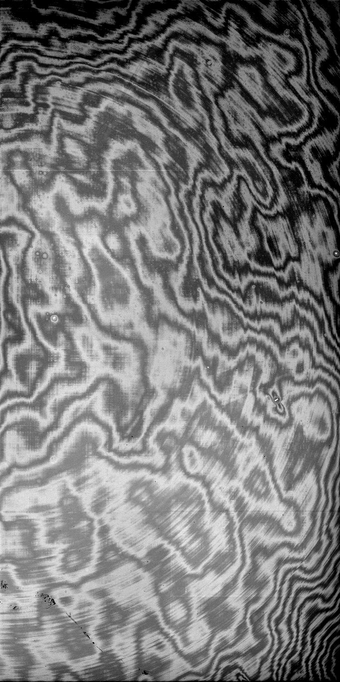
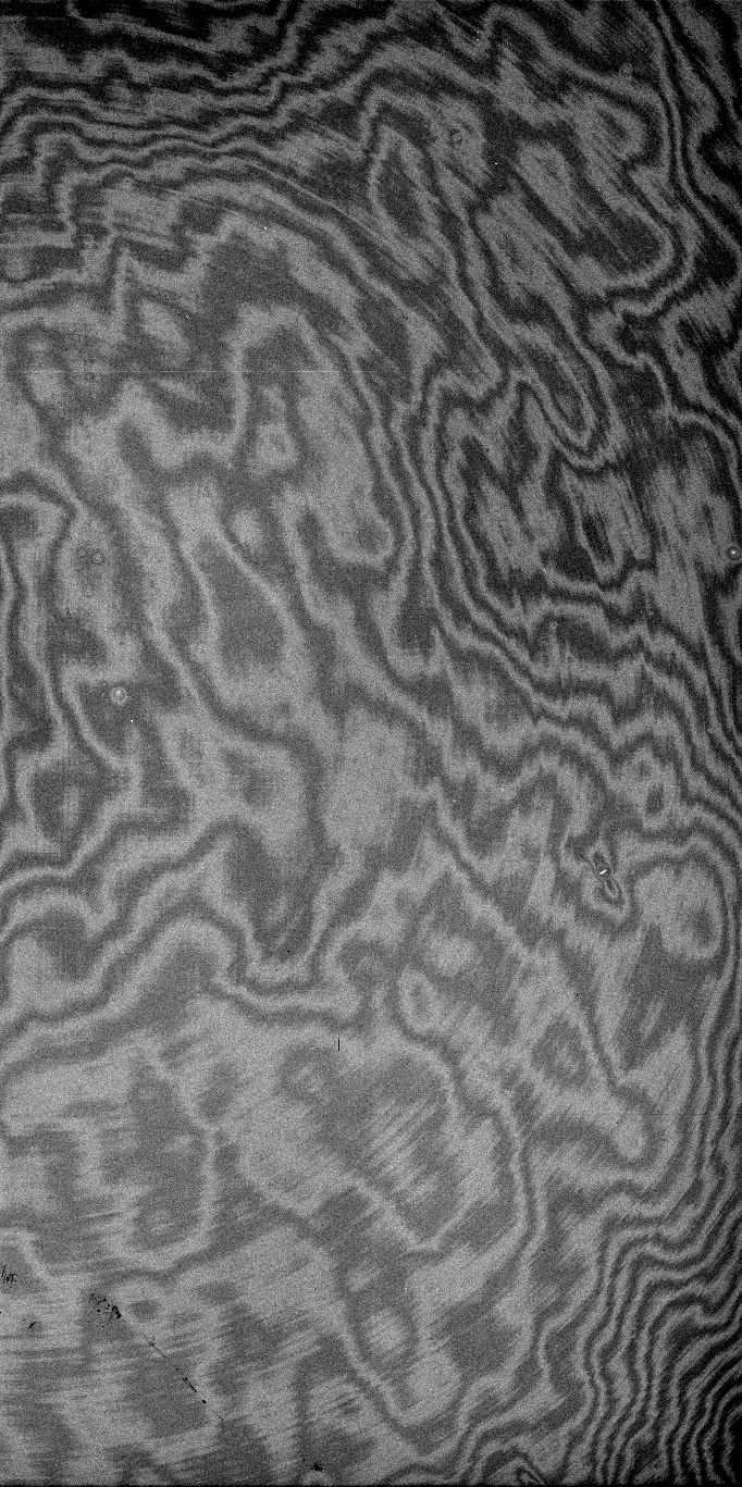
For the flat field we use three wavelengths, 350 nm, 600 nm and 900 nm. For each wavelength we make two images, high level (45000 ADU) and low level (1000 ADU).
350 nm (UV), bandwidth 5 nm |
600 nm, bandwidth 5 nm |
900 nm, bandwidth 5 nm |
|||
|
|
|
|
|
|
|
High level |
Low level |
High level |
Low level |
High level |
Low level |
Table 6: Flat field for three wavelengths.
The time exposure, for the long dark exposure, is 3600 seconds.
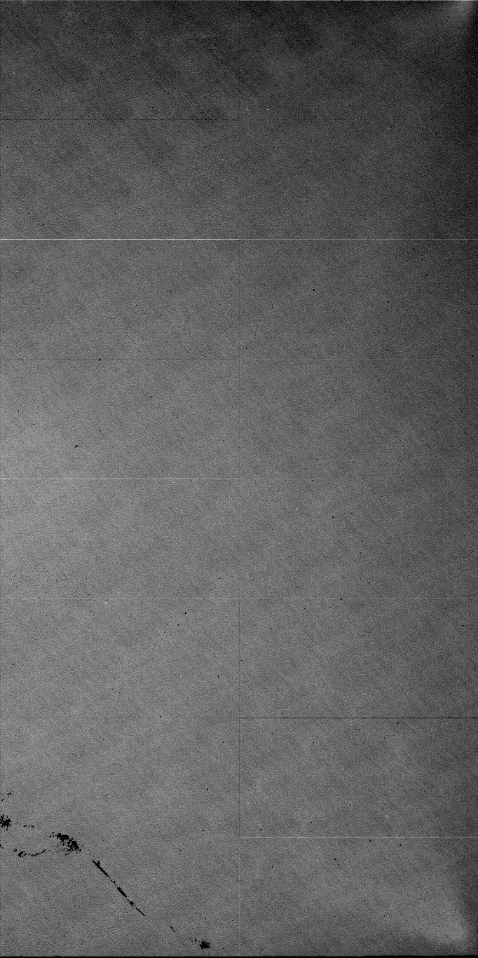
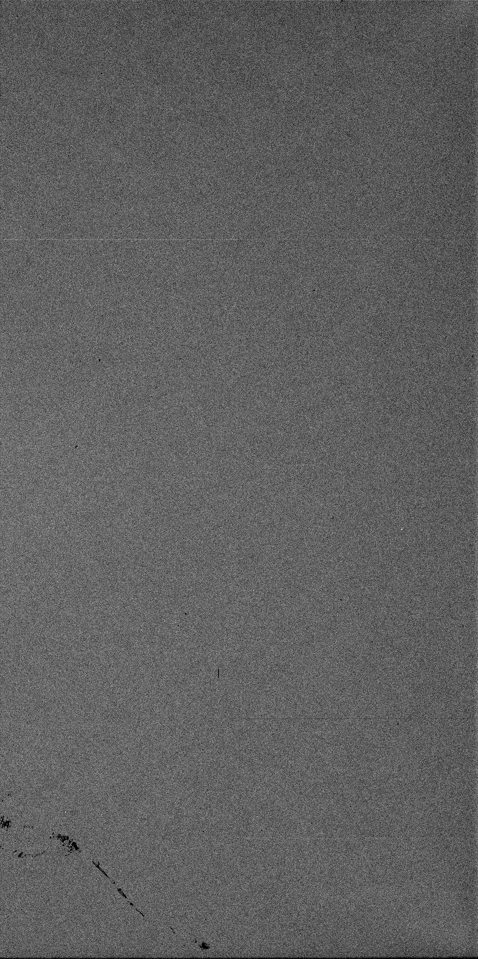
|
Bias |
Long exposure dark image |
|---|---|
|
|
|
Table 7: Bias and Dark.
Remark: As you can see on the dark image we have on this CCD some electroluminescence (two white spots below).
Clock mode: 225kpx/rr/HG/512
CCD Fornax, right port
Conversion Factor=   0.52794e-/ADU ±0.001899     for 20644.5ADU
RMS noise        =   3.309e-       ±0.1579

CCD Fornax, left port
Conversion Factor=   0.54125e-/ADU ±0.002398     for 20050.3ADU
RMS noise        =   3.4281e-      ±0.1591


Clock mode: 50kpx/rlrl/HG/512
CCD Fornax, left port
Conversion Factor=   0.5235e-/ADU  ±0.001772     for 20344.2ADU
RMS noise        =   2.8653e-      ±0.1381

CCD Fornax, right port
Conversion Factor=   0.50892e-/ADU ±0.001891     for 20731.9ADU
RMS noise        =   2.8974e-      ±0.1441
RMS non linearity (%)         = 0.27
Peak to peak non linearity (%)= 0.78

Figure 9: Error of linearity
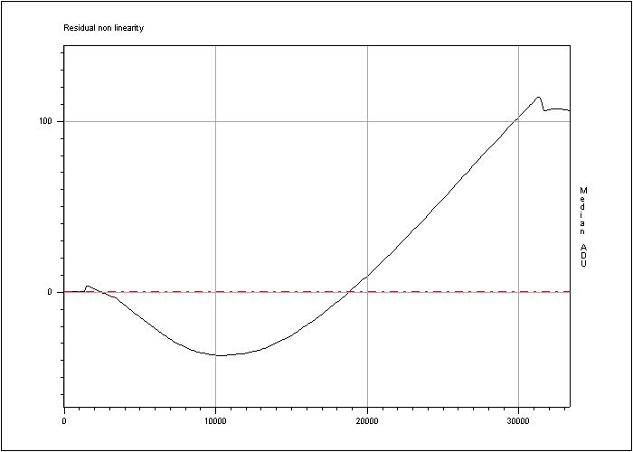
Figure 10: Residual non linearity.
Exposure time (s) = 3600, Temperature = -120 C

Dark current : 1.54 ± 0.07 ADU/hour/pixel
Dark current : 0.86 ± 0.04 e-/hour/pixel
Low level (Around 2500 ADU)
Horizontal CTE =
Vertical CTE   =

High level (Around 25000 ADU)
Horizontal CTE =
Vertical CTE   =
In this section we expose the hot pixel, the dark pixel, the trap and the very large trap we found.
A hot pixel provides a signal of > 60 e- / pixel / hour.
Result: 335 hot points.
a very bright pixel provides a signal of > 200000 e-/pixel/hour
Result: 0 very bright pixel.
A dark pixel is one with 50% or less than the average output for uniform intensity light level, measured with a flat field level around 500 photo-electrons.
Result: 23 dark pixels detected.
A trap is defined as a pixel that captures more than 10 electrons, measured with a flat field level around 500 photo-electrons.
Result: 14 trap
A very large trap is defined as a pixel that captures more than 10 000 electrons, measured with a flat field level around 90 % of full well capability.
Result: 1 very large trap.
Bad column
A bad column is 10 or more contiguous hot or dark pixels in a single column or a very bright pixel or a very large trap.
Result: bad columns.
Here is a summary of cosmetic defects:
|
|
Hot pixel |
Dark pixel |
A very bright pixel (a) |
Trap |
Very large trap (b) |
Sup. 10 contiguous pixels (c) |
Total bad column (a+b+c) |
|---|---|---|---|---|---|---|---|
|
ESO |
335 |
23 |
0 |
14 |
1 |
1 |
3 |
|
Marconi |
158 |
11 |
7 |
1 |
0 |
12 |
|
Table 8: Summary of cosmetic defects.
Remark: This CCD has not a clean surface and it is difficult to determine the cosmetic defects.
Back to the overview page ESO Test Reports for the OmegaCAM CCDs