|
|
|
|
|
|
Tucana |
: ESO CCD
Test Report |
|
|
|
|
|
|
|
| General
information |
|
|
| EEV
44-82-1-A57 |
|
NB - NB: Please note that the
correct CCD names are : |
|
| CCD
Name : |
Tucana |
|
| Grade : |
|
Science |
|
Tucana (serial no: 02395-20-01) and not Alcor as the data
files are called. |
|
| Serial
Number : |
02395-20-01 |
|
Triangulum Australe ( serial no: 02395-19-01) and not
Alcalurops as the data files are called. |
|
| Type
: Backside, Single layer AR Pixel size 15 x 15 μm |
|
| Number
of photosensitive pixels 2048 x 4102 [HxV] |
|
When the CCD's was tested they were given the wrong name
and therefor all the datafiles used |
|
| Number
of outputs : 2 |
|
this wrong name. Test reports etc. have a note about this
issue. |
|
| Overall
rating : |
|
|
| Measurement made by |
S.D. |
the |
2-Apr-2003 |
|
| Data reduced by |
|
JT |
the |
17-Apr-2003 |
|
|
| Setup |
|
|
D-Marc 1 |
|
| Position
in the head |
B |
|
| Tested
with the CCD |
Triangulum Australe |
|
|
| Concession
form |
/ |
|
|
| Volt table |
|
|
|
| Channel
voltage potential |
10.25 |
|
|
| This table defines
the voltages which will be applied to peripherals |
|
| at initialisation
time. It also defines the high and low limits which may |
|
| be set for these
voltages |
|
|
| BIASBRD is for the
EEV CCD-44 in the mosaic |
|
|
| # BRD_ID PERIPH_ID |
|
|
|
|
| # CONNECTOR
P0 - A |
|
|
|
|
LOW |
HIGH |
TOLERANCE |
INIT_VAL |
|
| BRD_ANABIAS0
ANB_PRESET_VOLT_A |
-3500 |
-1000 |
10000 |
-3500 |
#OG1R |
|
| BRD_ANABIAS0
ANB_PRESET_VOLT_B |
-2500 |
-1000 |
10000 |
-2500 |
#OG2R |
|
| BRD_ANABIAS0
ANB_PRESET_VOLT_C |
2000 |
25000 |
10000 |
22000 |
#ODR |
|
| BRD_ANABIAS0
ANB_PRESET_VOLT_D |
2000 |
15000 |
10000 |
11750 |
#RDR |
|
| BRD_ANABIAS0
ANB_PRESET_VOLT_E |
2000 |
25000 |
10000 |
25000 |
#JDR |
|
| BRD_ANABIAS0
ANB_PRESET_VOLT_F |
0 |
0 |
0 |
0 |
#not used |
|
| BRD_ANABIAS0
ANB_PRESET_VOLT_G |
0 |
0 |
0 |
0 |
#not used |
|
| BRD_ANABIAS0
ANB_PRESET_VOLT_H |
0 |
0 |
0 |
0 |
#not used |
|
|
|
|
| # CONNECTOR
PO - B |
|
|
|
|
LOW |
HIGH |
TOLERANCE |
INIT_VAL |
|
| BRD_ANABIAS0
ANB_PRESET_VOLT_I |
-3500 |
-1000 |
10000 |
-3500 |
#OG1L |
|
| BRD_ANABIAS0
ANB_PRESET_VOLT_J |
-2500 |
-1000 |
10000 |
-2500 |
#OG2L |
|
| BRD_ANABIAS0
ANB_PRESET_VOLT_K |
2000 |
25000 |
10000 |
22000 |
#ODL |
|
| BRD_ANABIAS0
ANB_PRESET_VOLT_L |
2000 |
15000 |
10000 |
11750 |
#RDL |
|
| BRD_ANABIAS0
ANB_PRESET_VOLT_M |
2000 |
25000 |
10000 |
25000 |
#JDL |
|
| BRD_ANABIAS0
ANB_PRESET_VOLT_N |
0 |
0 |
0 |
0 |
#not used |
|
| BRD_ANABIAS0
ANB_PRESET_VOLT_O |
2000 |
19000 |
10000 |
18000 |
#DDLR |
|
| BRD_ANABIAS0
ANB_PRESET_VOLT_P |
0 |
0 |
0 |
0 |
#not used |
|
|
|
|
|
|
|
| #The
anabias board also has an opto isolated peripheral |
|
|
|
|
|
| BRD_ANABIAS0
ANB_OPTOOUT |
0 |
32767 |
4 |
255 |
|
|
| CLOCKDRIVER
BOARD 0 is for the EEV CCD44 in the mosaic |
|
|
|
| # BRD_ID PERIPH_ID |
|
|
|
|
|
| # CONNECTOR PO-A |
|
|
|
|
LOW |
HIGH |
TOLERENCE |
INIT_VAL |
|
| BRD_CLKDRV0
CLKDRV_DAC0_LO |
-5000 |
-5000 |
1000 |
-5000 |
#SWL |
|
| BRD_CLKDRV0
CLKDRV_DAC0_HI |
5000 |
5000 |
1000 |
5000 |
|
|
| BRD_CLKDRV0
CLKDRV_DAC1_LO |
-5000 |
-5000 |
1000 |
-5000 |
#SWR |
|
| BRD_CLKDRV0
CLKDRV_DAC1_HI |
5000 |
5000 |
1000 |
5000 |
|
|
| BRD_CLKDRV0
CLKDRV_DAC2_LO |
-5000 |
-5000 |
1000 |
-5000 |
#RF3 |
|
| BRD_CLKDRV0
CLKDRV_DAC2_HI |
5000 |
5000 |
1000 |
5000 |
|
|
| BRD_CLKDRV0
CLKDRV_DAC3_LO |
-5000 |
-5000 |
1000 |
-5000 |
#RF2L |
|
| BRD_CLKDRV0
CLKDRV_DAC3_HI |
5000 |
5000 |
1000 |
5000 |
|
|
| BRD_CLKDRV0
CLKDRV_DAC4_LO |
-5000 |
-5000 |
1000 |
-5000 |
#RF1L |
|
| BRD_CLKDRV0
CLKDRV_DAC4_HI |
5000 |
5000 |
1000 |
5000 |
|
|
| BRD_CLKDRV0
CLKDRV_DAC5_LO |
-5000 |
-5000 |
1000 |
-5000 |
#RF2R |
|
| BRD_CLKDRV0
CLKDRV_DAC5_HI |
5000 |
5000 |
1000 |
5000 |
|
|
| BRD_CLKDRV0
CLKDRV_DAC6_LO |
-5000 |
-5000 |
1000 |
-5000 |
#RF1R |
|
| BRD_CLKDRV0
CLKDRV_DAC6_HI |
5000 |
5000 |
1000 |
5000 |
|
|
| BRD_CLKDRV0
CLKDRV_DAC7_LO |
-6000 |
-6000 |
1000 |
-6000 |
#DG |
|
| BRD_CLKDRV0
CLKDRV_DAC7_HI |
6000 |
6000 |
1000 |
6000 |
|
|
|
|
|
| # CONNECTOR PO-B |
|
|
|
|
LOW |
HIGH |
TOLERENCE |
INIT_VAL |
|
| BRD_CLKDRV0
CLKDRV_DAC8_LO |
-12000 |
-4000 |
1000 |
-8000 |
#IF1 |
|
| BRD_CLKDRV0
CLKDRV_DAC8_HI |
-2000 |
3000 |
1000 |
2000 |
|
|
| BRD_CLKDRV0
CLKDRV_DAC9_LO |
-12000 |
-4000 |
1000 |
-8000 |
#IF2 |
|
| BRD_CLKDRV0
CLKDRV_DAC9_HI |
-2000 |
3000 |
1000 |
2000 |
|
|
| BRD_CLKDRV0
CLKDRV_DAC10_LO |
-12000 |
-4000 |
1000 |
-8000 |
#IF3 |
|
| BRD_CLKDRV0
CLKDRV_DAC10_HI |
-2000 |
3000 |
1000 |
2000 |
|
|
| BRD_CLKDRV0
CLKDRV_DAC11_LO |
0 |
0 |
1000 |
0 |
#empty |
|
| BRD_CLKDRV0
CLKDRV_DAC11_HI |
0 |
0 |
1000 |
0 |
|
|
| BRD_CLKDRV0
CLKDRV_DAC12_LO |
-6000 |
-4000 |
1000 |
-6000 |
#FRL |
|
| BRD_CLKDRV0
CLKDRV_DAC12_HI |
6000 |
8000 |
1000 |
6000 |
|
|
| BRD_CLKDRV0
CLKDRV_DAC13_LO |
-6000 |
-4000 |
1000 |
-6000 |
#FRR |
|
| BRD_CLKDRV0
CLKDRV_DAC13_HI |
6000 |
8000 |
1000 |
6000 |
|
|
|
| # |
|
| # Gain
should be interpreted as follows |
|
| # There
are two gains, gain1 is on the preamp, gain2 is on the video board. |
|
|
| # Gain1 = |
|
| #
3 == 1.5 |
|
| #
1 == 2.25 |
|
| #
0 == 3.0 |
|
| # |
|
| # Gain2
= |
|
| # 0 = Minimum
(2.5) |
|
| # 1 = Maximum
(12.5) |
|
| # |
|
| # BRD_ID PERIPH_ID |
LOW |
HIGH |
TOLERANCE |
INIT_VAL |
|
| BRD_VIDBRD0
VID_GAIN1_CHAN0 |
0 |
3 |
0 |
1 |
|
| BRD_VIDBRD0
VID_GAIN1_CHAN1 |
0 |
3 |
0 |
1 |
|
| BRD_VIDBRD0
VID_GAIN1_CHAN2 |
0 |
3 |
0 |
1 |
|
| BRD_VIDBRD0
VID_GAIN1_CHAN3 |
0 |
3 |
0 |
1 |
|
|
|
|
| BRD_VIDBRD0
VID_GAIN2_CHAN0 |
0 |
1 |
0 |
0 |
|
| BRD_VIDBRD0
VID_GAIN2_CHAN1 |
0 |
1 |
0 |
0 |
|
| BRD_VIDBRD0
VID_GAIN2_CHAN2 |
0 |
1 |
0 |
0 |
|
| BRD_VIDBRD0
VID_GAIN2_CHAN3 |
0 |
1 |
0 |
0 |
|
|
|
|
| BRD_VIDBRD0
VID_FILT_CHAN0 |
0 |
3 |
0 |
0 |
|
| BRD_VIDBRD0
VID_FILT_CHAN1 |
0 |
3 |
0 |
0 |
|
| BRD_VIDBRD0
VID_FILT_CHAN2 |
0 |
3 |
0 |
0 |
|
| BRD_VIDBRD0
VID_FILT_CHAN3 |
0 |
3 |
0 |
0 |
|
|
|
|
| BRD_VIDBRD0
VID_TESTVID_CHAN0 |
0 |
1 |
0 |
0 |
|
| BRD_VIDBRD0
VID_TESTVID_CHAN1 |
0 |
1 |
0 |
0 |
|
| BRD_VIDBRD0
VID_TESTVID_CHAN2 |
0 |
1 |
0 |
0 |
|
| BRD_VIDBRD0
VID_TESTVID_CHAN3 |
0 |
1 |
0 |
0 |
|
|
| # Video Offsets are
in 0.001 volts |
|
|
| # BRD_ID PERIPH_ID |
LOW |
HIGH |
TOLERANCE |
INIT_VAL |
|
| BRD_VIDBRD0
VID_OFFSET_CHAN0 |
0 |
65535 |
6553 |
0 |
|
| BRD_VIDBRD0
VID_OFFSET_CHAN1 |
0 |
65535 |
6553 |
0 |
|
| BRD_VIDBRD0
VID_OFFSET_CHAN2 |
0 |
65535 |
6553 |
0 |
|
| BRD_VIDBRD0
VID_OFFSET_CHAN3 |
0 |
65535 |
6553 |
0 |
|
|
| Quantum
Efficiency |
|
|
| Clock mode : |
225kpx/rr/HG/512 |
|
| Conversion factor |
1.0697e-/ADU |
±0.005578 |
for |
23618.1ADU |
|
| Rms noise : |
5.2794e- |
±0.03948 |
|
|
| CCD Temperature : |
-120.2Cº |
|
|
|
Wav. |
QE% |
QE error |
PRNU rms% |
|
Wav. |
QE% |
QE error |
PRNU rms% |
|
|
300 |
29.4 |
0.1 |
2.3 |
|
660 |
75.3 |
0.0 |
1.0 |
|
|
310 |
46.1 |
0.0 |
2.0 |
|
680 |
73.2 |
0.0 |
1.0 |
|
|
320 |
45.8 |
0.0 |
1.9 |
|
700 |
70.2 |
0.3 |
1.0 |
|
|
330 |
48.1 |
0.0 |
1.8 |
|
720 |
67.2 |
0.0 |
1.0 |
|
|
340 |
49.6 |
0.0 |
1.8 |
|
740 |
63.5 |
0.0 |
1.0 |
|
|
350 |
50.1 |
0.0 |
1.8 |
|
750 |
61.4 |
0.0 |
1.0 |
|
|
360 |
50.6 |
0.0 |
1.8 |
|
760 |
59.3 |
0.0 |
1.1 |
|
|
370 |
54.7 |
0.1 |
1.5 |
|
780 |
54.7 |
0.0 |
1.1 |
|
|
380 |
63.7 |
0.1 |
1.3 |
|
800 |
50.3 |
0.0 |
1.1 |
|
|
390 |
70.9 |
0.1 |
1.1 |
|
820 |
46.0 |
0.0 |
1.1 |
|
|
400 |
75.8 |
0.1 |
1.1 |
|
840 |
41.7 |
0.0 |
1.1 |
|
|
420 |
80.7 |
0.0 |
1.0 |
|
850 |
39.2 |
0.0 |
1.1 |
|
|
440 |
82.6 |
0.1 |
1.0 |
|
860 |
36.6 |
0.0 |
1.1 |
|
|
450 |
82.8 |
0.0 |
1.0 |
|
880 |
31.2 |
0.0 |
1.1 |
|
|
460 |
82.9 |
0.0 |
1.0 |
|
900 |
25.8 |
0.0 |
1.4 |
|
|
480 |
82.5 |
0.0 |
1.0 |
|
920 |
20.0 |
0.0 |
1.4 |
|
|
500 |
81.8 |
0.1 |
1.0 |
|
940 |
15.0 |
0.0 |
1.7 |
|
|
520 |
81.2 |
0.0 |
1.0 |
|
950 |
12.8 |
0.0 |
1.5 |
|
|
540 |
80.5 |
0.0 |
1.0 |
|
960 |
10.6 |
0.0 |
1.4 |
|
|
550 |
80.3 |
0.0 |
1.0 |
|
980 |
6.9 |
0.0 |
1.2 |
|
|
560 |
80.0 |
0.0 |
1.0 |
|
1000 |
4.0 |
0.0 |
1.4 |
|
|
580 |
79.5 |
0.0 |
1.0 |
|
1020 |
1.9 |
0.0 |
1.7 |
|
|
600 |
78.8 |
0.0 |
1.0 |
|
1040 |
0.7 |
0.0 |
2.2 |
|
|
620 |
77.9 |
0.0 |
1.0 |
|
1060 |
0.3 |
0.0 |
2.8 |
|
|
640 |
76.8 |
0.0 |
1.0 |
|
1080 |
0.2 |
0.0 |
3.1 |
|
|
650 |
76.1 |
0.0 |
1.0 |
|
1100 |
0.1 |
0.0 |
4.1 |
|
|
|
Table 1: Measurements of the quantum efficiency and PRNU |
|
|
| Quantum
efficiency, comparison |
|
|
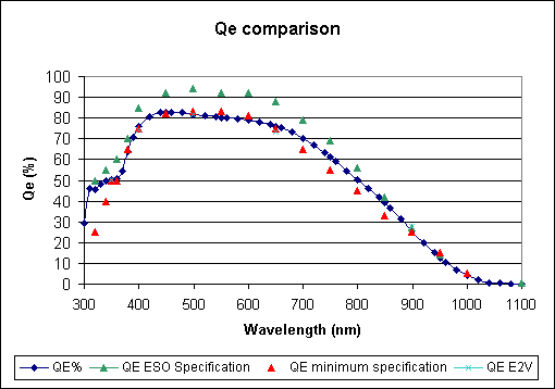
| In this section you
can compare the QE we measured with the testbench and: |
|
|
|
l QE Minimum specification |
|
|
l Typical QE |
|
|
l QE from Marconi |
|
|
|
|
|
|
|
|
|
|
|
|
|
|
|
|
|
|
|
|
|
|
|
|
|
|
|
|
|
|
|
|
|
|
|
|
|
|
|
|
|
|
|
|
|
|
|
|
|
|
|
|
|
|
|
|
|
|
|
|
|
|
|
|
|
|
|
|
|
Figure 1: Comparison between the QE measured by ESO, the QE measured
by Marconi, ESO specification and minimum specification |
|
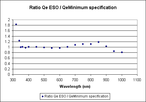
Figure 2: Ratio between the ESO measurements and the ESO minimum
specification |
|
|
|
|
| Quantum
efficiency, special specification |
|
|
|
Special
specification |
|
|
Wavelength
(nm) |
Minimum
spec.(%) |
ESO measure.
(%) |
Result |
|
|
350 |
50 |
50.1 |
OK |
|
|
400 |
80 |
75.8 |
Under the minimum
spec. |
|
|
650 |
80 |
76.1 |
Under the minimum
spec. |
|
|
900 |
25 |
25.8 |
OK |
|
|
Conclusion: |
No
this ccd is not in the 25% |
|
|
|
Table 2: Minimum specification for 25% of the ccds. |
|
|
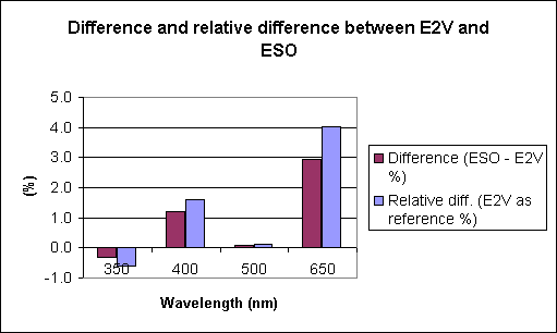
| Difference
between QE measurements made by ESO and Marconi |
|
|
|
Comparison
QE ESO and Marconi |
|
|
Wavelength
(nm) |
QE
ESO (%) |
QE
E2V (%) |
Difference
(ESO - E2V %) |
Relative
diff. (E2V as reference %) |
Ratio
QE ESO / QE E2V |
|
|
|
|
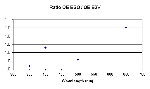
350 |
50.1 |
50.4 |
-0.3 |
-0.6 |
1.0 |
|
|
400 |
75.8 |
74.6 |
1.2 |
1.6 |
1.0 |
|
|
500 |
81.8 |
81.7 |
0.1 |
0.1 |
1.0 |
|
|
650 |
76.1 |
73.1 |
3.0 |
4.0 |
1.0 |
|
|
|
Table 3: Difference and relative difference between ESO measurements
and E2V |
|
|
|
|
|
|
|
|
|
|
|
|
|
|
|
|
|
|
|
|
|
|
|
|
|
|
|
|
|
|
|
|
|
|
|
|
|
|
|
|
|
|
|
|
|
|
|
|
|
|
|
|
|
|
|
|
|
|
|
|
Figure 3: Graphic representation of the fdifference and the relative
difference |
|
Figure 4: Ration between the ESO measurements and the E2V Measurements |
|
|
|
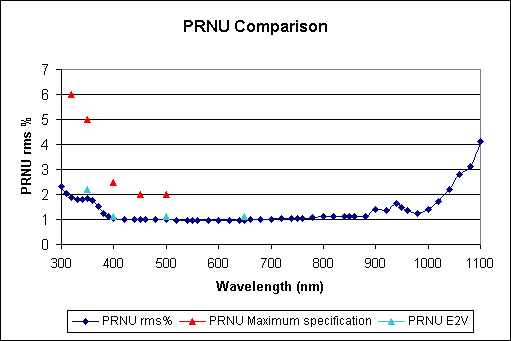
| PRNU comparison |
|
|
| In this section you
can compare the PRNU we measured at ESO and: |
|
|
|
l PRNU Minimum specification |
|
|
l PRNU from Marconi |
|
|
|
|
|
|
|
|
|
|
|
|
|
|
|
|
|
|
|
|
|
|
|
|
|
|
|
|
|
|
|
|
|
|
|
|
|
|
|
|
|
|
|
|
|
|
|
|
|
|
|
|
|
|
|
|
|
|
|
|
|
|
|
|
|
|
Figure 5: Comparison between the PRNU measured by ESO, the PRNU measured
by Marconi, and the maximum specification |
|
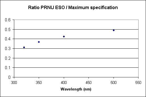
Figure 6: Ratio between the ESO measurements and the maximum specification |
|
|
|
|
|
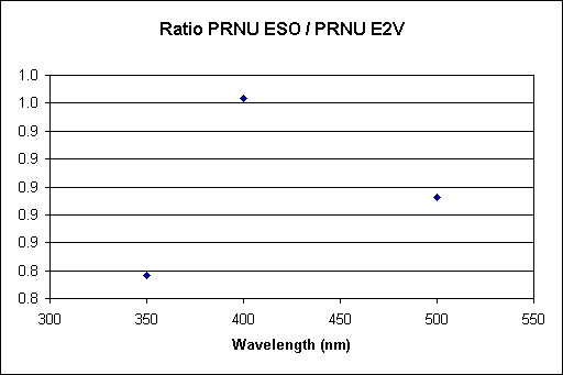
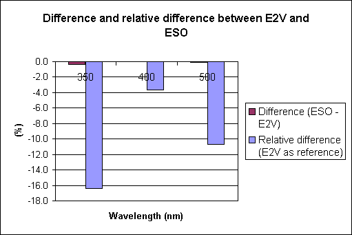
Comparison
PRNU ESO and PRNU Marconi |
|
|
Wavelength
(nm) |
PRNU
ESO (rms %) |
Maximum
spec. |
PRNU
E2V |
Difference
(ESO - E2V) |
Relative
difference (E2V as reference) |
Ratio
PRNU ESO / PRNU E2V |
|
|
|
|
320 |
1.9 |
6.0 |
/ |
/ |
/ |
/ |
|
|
350 |
1.8 |
5.0 |
2.2 |
-0.4 |
-16.4 |
0.8 |
|
|
400 |
1.1 |
2.5 |
1.1 |
0.0 |
-3.6 |
1.0 |
|
|
500 |
1.0 |
2.0 |
1.1 |
-0.1 |
-10.7 |
0.9 |
|
|
|
Table 4: difference and relative difference between ESO and E2V
measurements |
|
|
|
|
|
|
|
|
|
|
|
|
|
|
|
|
|
|
|
|
|
|
|
|
|
|
|
|
|
|
|
|
|
|
|
|
|
|
|
|
|
|
|
|
|
|
|
| Comparison
with the contract |
|
|
| In this section
you will see the if the values we have measured for the QE and the PRNU
are in accordance with the contract. |
|
|
|
Wavelength
(nm) |
QE |
PRNU |
|
|
320 |
OK |
OK |
|
|
340 |
OK |
/ |
|
|
350 |
OK |
OK |
|
|
360 |
OK |
/ |
|
|
380 |
Below
the specification |
/ |
|
|
400 |
OK |
OK |
|
|
450 |
OK |
OK |
|
|
500 |
Below
the specification |
OK |
|
|
550 |
Below
the specification |
/ |
|
|
600 |
Below
the specification |
/ |
|
|
650 |
OK |
/ |
|
|
700 |
OK |
/ |
|
|
750 |
OK |
/ |
|
|
800 |
OK |
/ |
|
|
850 |
OK |
/ |
|
|
900 |
OK |
/ |
|
|
950 |
Below
the specification |
/ |
|
|
1000 |
Below
the specification |
/ |
|
|
|
Table 5: Comparison between the values we have measured and the
specifications in the contract |
|
|
| Cosmetic |
|
|
| Click here to see the images |
|
|
| Cosmetic
defects |
|
|
| In this section
we expose the hot pixel, the dark pixel, the trap and the very large trap
we have found. |
|
|
| Hot
pixel |
A hot
pixel provides a signal of > 60 e- / pixel
/ hour. |
|
|
|
| Very
bright pixel |
a very bright pixel provides
a signal of > 200000 e-/pixel/hour |
|
|
|
| Dark
pixel |
A dark pixel is one with 50% or less than the average output for uniform
intensity light level, measured with a flat field level around 500 photo-electrons |
|
|
|
| Trap |
A trap is defined as a pixel that captures more than 10 electrons,
measured with a flat field level around 500 photo-electrons. |
|
|
|
| Very
large trap |
A very large trap is defined as a pixel that captures more than 10 000 electrons,
measured with a flat field level around 90% of full well capability. |
|
|
|
| Bad
column |
A bad column is 10 or more contiguous hot
or dark pixels in a single column or a very bright pixel or a very large trap. |
|
|
|
|
|
|
|
|
Hot
pixel |
Dark
pixel |
Very
bright pixel (a) |
Trap |
Very
large trap (b) |
Sup.
10 contiguous pixels (c) |
Total
bad column (a+b+c) |
|
|
|
|
ESO |
1 |
12 |
0 |
3 |
0 |
13 |
13 |
|
|
E2V |
4 |
0 |
3 |
0 |
2 |
2 |
|
|
|
Table 6: Cosmetic defects measured by ESO and E2V |
|
|
| Dark and
Bias |
|
|
| Click here to see the images |
|
|
| Readout
noise and conversion factor |
|
|
| Conversion factor,
recommend specification: |
0.55 |
e-/pixel/hour |
|
| Maximum readout noise
at 50kpix/s: |
2 |
e- |
|
| Maximum readout noise
at 225kpix/s: |
2.8 |
e- |
|
|
|
Conversion
factor |
Readout
noise |
|
|
50kpix/s |
Left port |
0.51 |
2.64 |
|
|
Right port |
0.51 |
2.64 |
|
|
225kpix/s |
Left port |
0.52 |
5.52 |
|
|
Right port |
0.53 |
5.43 |
|
|
|
Table 7: Readout noise and Conversion factor measured at 50 and
225kpix/s |
|
|
| Linearity |
|
|
| Minimum
specification: |
1 |
(%) |
|
|
|
Rms
non linearity (%) |
0.24 |
|
|
Peak
to peak non linearity (%) |
0.70 |
|
|
|
Table 8: Linearity |
|
|
| Click here to see the graphics |
|
|
| Dark current |
|
| Exposure
time (s): |
3600 |
|
| Readout
mode: |
50kpix/s |
|
| Port: |
Right |
|
|
|
|
| Minimum
specification: |
2 |
e-/pixel/hour |
|
|
|
Dark
current |
error |
|
|
0.69 |
0.24 |
ADU/pixel/hour |
|
|
0.35 |
0.12 |
e-/pixel/hour |
|
|
|
Table 9: Dark current in electron per pixel and per hour |
|
|
| Charge
Transfer Efficiency (CTE) |
|
|
| Method
used: |
EPER |
|
|
|
|
| Minimum
specification: |
0.999995 |
|
|
|
CTE (ESO) |
CTE
(E2V) |
|
|
CTE
Serial (Horizontal) Left |
0 |
0.999995 |
|
|
CTE
Serial (Horizontal) Right |
0.999996 |
0.999995 |
|
|
CTE
Parallel (Vertical) |
0.999999 |
0.999998 |
|
|
|
Table 10: Charge transfer efficiency measured at 50 kpix/s and the
high gain amplification |
|
|
|
|
|
|
|
|
|
|
|
|
|
|
|
|
|
|
|
|
|
|