
FIERA
James W. Beletic, Rolf Gerdes and Raymond C. DuVarney
(Updated by Javier Reyes in March 2004)
Abstract
ESO developed a new generation CCD controller for the Very Large Telescope (VLT) facility on Cerro Paranal. This CCD controller, named FIERA, is also used at the Cerro La Silla Observatory and in ESO´s testing and integration laboratories. A major emphasis in the FIERA design is the ability to run a large number of CCD outputs at fast readout rates, so as to take advantage of the new generation of high speed, low noise amplifiers. The first FIERA prototype was successfully demonstrated in October 1996. The design underwent an upgrade during 2000 and about 20 systems have been produced so far and successfully deployed through the facilities.
1. Motivation for FIERA development
The quality of CCD detectors continues to improve. CCDs are getting larger (the new standard is 2k x 4k and sizes up to 9k x 9k are being made) and high quantum efficiency devices, with peak q.e. greater or equal than 90 %, are now produced for all advanced instruments. Another significant advance in CCD technology is the development of high speed, low noise readout amplifiers. Two examples are:
- The MIT/LL amplifier which achieves 4-6 e- at 1000 kps (i.e. 1 MHz), ≤ 2 e- noise at 100 kps, and ~ 1 e- at 20 kps,
- The EEV amplifier which achieves about 6 e- at 1000 kps and less than, or equal to 3 e- at 50 kps.
The combination of large CCDs and the new amplifiers generated back in 1995 a need for CCD controllers that could read many ports in parallel at high speed. The motivation for short readout times is often due to the impatience of a waiting astronomer, but there are more important reasons for high speed, low noise readout:
- Time is money. It costs about 1 Euro (~1US $) per second to operate an 8-meter class telescope. Reducing readout time of large mosaics from periods of minutes to 10 seconds will save the equivalent of the cost of the CCD controller every few months, on every instrument.
- A large fraction of telescope data can be read out at 1000 kps and 6 e- noise without any degradation to the data quality. This category includes acquisition, focusing, flat-fields, calibration spectra, high light level spectra and nearly all direct sky imaging.
- Fast frame rate imaging will allow new kinds of science to be done (e.g. fast photometry of rapidly varying objects) and is mandatory for adaptive optics systems.
As ESO concentrated its CCD procurement on new generation amplifiers, in parallel we developed a CCD controller able to take full advantage of the speed possible with these CCDs.
That was also an ideal time for ESO to develop and deploy a new generation CCD controller. Starting in 1998, ESO began the commissioning of the Very Large Telescope (VLT) on Cerro Paranal in Chile. This facility consists of four 8.2 meter telescopes with three 1.8 meter auxiliary telescopes for interferometry. Each of the 8.2-m telescopes has 3 main foci (Cassegrain and 2 Nasmyth) and also a Coudé feed, which means there is a need for a large number of optical detector systems.
Since the VLT control system is a very large software system within which the CCD controllers operate, it was important to develop and maintain a well-defined interface. To provide the highest reliability and to minimize maintenance, it was decided to use a single controller for all scientific CCD systems.
By taking this approach, for slow readout CCDs, the "universal" controller was overbuilt and did not make use of all of its higher priced components. However, we were certain (and our experience has not proven otherwise) that the savings in development, deployment and maintenance would more than offset the total component cost.
It was also wished to be prepared for the "next generation" amplifiers as there were efforts to make amplifiers that would be only 1 to 2 e- noise at 1000 kps, and such amplifiers would achieve sub-electron noise at 100 kps. (This type of performance was demonstrated nearly a decade ago ([2]).) In addition, since the CCD controller should have a lifetime of at least 10-15 years, it had be designed to easily integrate the coming generation of ultra-low noise CCD amplifiers.
We named our controller FIERA, which is an acronym for Fast Imager Electronic Readout Assemby. As the CCD systems would primarily reside in Chile, it was appropriate that FIERA means "wild animal" in Spanish; an apt description of this controller, for which no holds were barred in the name of speed and flexibility.
2. FIERA Design Philosophy
The overriding design philosophy for FIERA was that it should be transparent to the user. That is, the performance of the entire CCD system should be limited only by the CCD and the imagination of the user.
Also, as stated above, FIERA should be a universal controller to be used for every CCD or mosaic in ESO’s instruments. This includes the following list of CCDs and mosaics:
- Tektronix / SITe 2k x 2k - 4 port
- VLT Test Camera CCD, which is a custom (Loral) designed 2k x 2k, 4 port device with 4 single port tracker chips located at the 4 corners (see Fig. x of [1], to see a photo of the CCD),
- 4k x 4k mosaic of two 2k x 4k CCDs - total of 4 ports,
- 8k x 8k mosaic of eight 2k x 4k CCDs - total of 8 or 16 ports used,
- 128 x 128 split frame adaptive optics CCD - 16 ports, all of which must be read at speeds to 1 million pixels per port per second (1000 kps),
- Mosaic of thirty-two 2k x 4k devices, meaning 32 or 64 readout ports that could be controlled by two FIERAs running synchronously.
FIERA run relatively slowly with the Tektronix, SITe and Loral CCDs, but had to run at 1000 kps for the mosaics of 2k x 4k devices. For the larger mosaics and the adaptive optics CCD, at least 16 ports need to be read out at speeds to at least 1000 kps. This meant that FIERA had to be able to handle at least 16 million pixels per second peak data rates.
In addition, FIERA was conceived to have the following qualities:
- synchronous timing of all signals,
- fully deterministic generation of all signals, no random timing of processor operating software should be involved,
- use standard commercial ("off the shelf") components as much as possible,
- no software in the detector head electronics, implementing almost all software in the embedded computer using C and C++,
- design / use lifetime of at least 15 years,
- use of industry standard components, shying away from some components that may not be available on the market in a few years time,
- modular design so that some aspects (e.g. video signal processing) can be upgraded at a future date for better design or to overcome the unavailability of specific components,
- easy to program and adapt to different CCD systems,
- ability to run standalone, within the VLT control system or operate at the non-VLT standard telescopes of La Silla,
- as simple as possible
Of course, we also required FIERA to have system noise that is negligible relative to the CCD noise, to be linear to better than 0.5% over the dynamic range of the A/D, to have no pattern noise, and to have crosstalk between video channels which is less than 1 part in 100,000 (for 16 bit A/D converters).
Note that there are two major items missing from the above list of qualities for FIERA: (a) small size, and (b) low power. For all of the planned ESO systems, size and power usage were not strong constraints and thus we did not impose them on our design. For removal of heat, the FIERA system uses liquid cooling to satisfy the VLT temperature requirement (outside of the electronics housing within 1.5 degrees of ambient air temperature).
Example of FIERA System driving 16 output video channels for NAOS chip.
3. Hardware Overview
With the above requirements in hand, the FIERA design process was initiated in 1995 by the three authors of this paper. During 1996, significantly more resources were put to the task, and in October 1996 a prototype was tested demonstrating that the design philosophy and implementation approach were both valid.
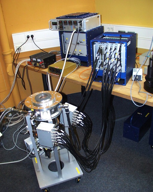
An overview of the FIERA hardware design is shown in Fig. 1 and a summary of the system specifications are given in Table 1. There are five main components:
- Embedded computer with auxiliary boards for sequence timing, data capture and network connection to other computers (monitor and keyboard are optional).
- Detector head electronics with clock drivers, analog bias generation and video signal processing.
- CCD detector head with pre-amplifier circuitry.
- PULPO housekeeping box for temperature control, vacuum sensing and shutter control.
- DC power supply module to generate the 5, ± 15, 24 and 30 V DC power needed by the detector head electronics and PULPO
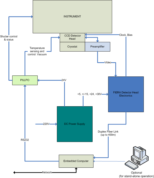
Figure. 1 Overview of the main components of the FIERA CCD controller system.
Also shown in Fig. 1 is the LN2 cryostat for cooling the CCDs, but that is not considered part of the FIERA system. Typically, all of these components are mounted at the instrument and the connection to the telescope control room is via the network connection from the embedded computer. However, in some cases, the embedded computer is placed either in the control room, or in a rack which is located on the Nasmyth platform or telescope floor.
Fundamental clock frequency |
50 MHz |
Number of readout channels |
Up to 32 |
Maximum total pixel rate |
50 million pixels/sec |
Number of bits/pixel |
Up to 21 (initially 16, set by A/D) |
Maximum speed / port |
5.5 million pixels/sec |
Clock drivers |
Fully programmable |
|
(25.6 V swing, 0.1 V resolution, 2 A current) |
Number of control bits |
virtually unlimited |
Analog biases |
fully programmable |
|
with hardware limits for CCD protection |
Gain settings |
6 (3 on the pre-amplifier and 2 on the video board) |
Filtering settings |
4 (for different readout rates) |
Offset levels |
64k levels - each channel indiv. programmable |
Data link |
Gigabit/sec from detector head |
|
to computer (up to 400m long) |
Telemetry |
All voltages remotely readable |
Test signals |
Synthetic video generation |
Software in the detector head |
None - all in C, C++ in the |
|
embedded computer |
Modularity |
Separate modules allowing |
|
upgrades and expandability |
Table 1. System specifications for the FIERA CCD controller
3.1 Embedded computer
Figure 2 shows the architecture of the embedded computer and the detector head electronics. The CPU power of the embedded computer is provided by a SPARCstation which contains the control software, all written in C and C++. This embedded computer is a combination of commercially available components and a custom designed Detector Electronics Interface Board. The interface board contains a Texas Instruments DSP (Digital Signal Processor), the TMS320C40, which provides the accurately timed generation of sequencer commands. See Figure 2a . The interface board includes a duplex gigabit fiber optic link based on the Finisar transceiver. We use a Hewlett-Packard HDMP module to serialize the digital data stream, providing 21 bit wide words at 50 million words per second.
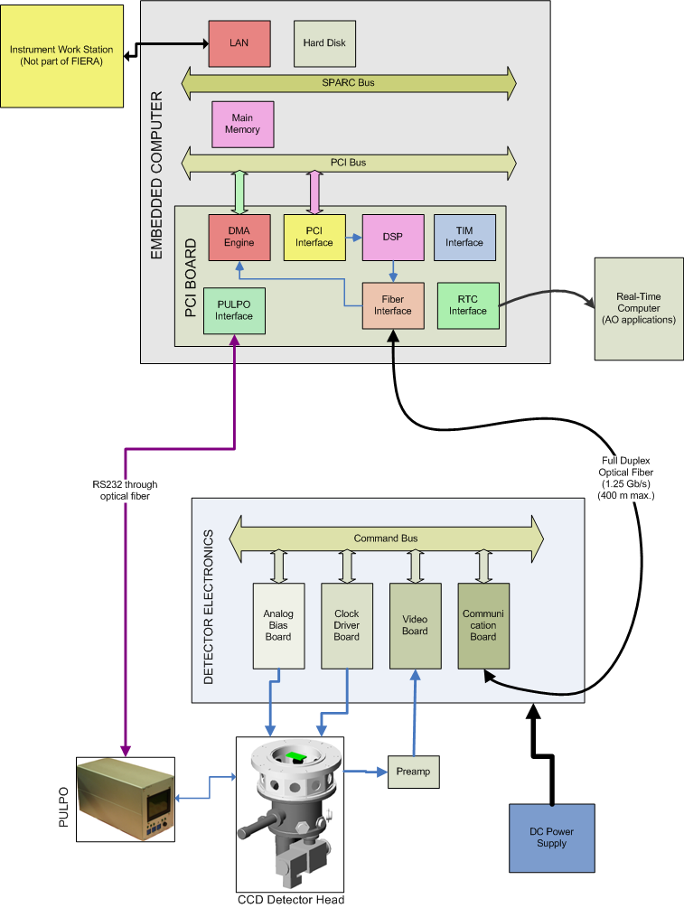
Figure 2a: FIERA hardware architecture showing printed circuit boards of the embedded computer and the detector head electronics.
For the detector head control, two words are used to send commands "up" the data link to the detector head electronics (thus commands are sent at 40 nsec time boundaries, same as the global bus output of the C40). To transfer data from the detector head "down" to the embedded computer, there are 21 bits per pixel. At present, 16 bits are used for data and 5 bits for readout port number, but the system was designed to be easily adapted to handle greater precision, up to 21 bits for data, in case the video signal processing chain evolved to produce such data.
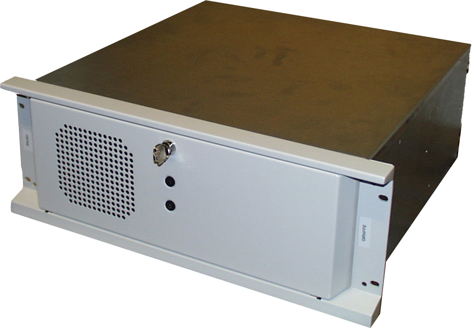
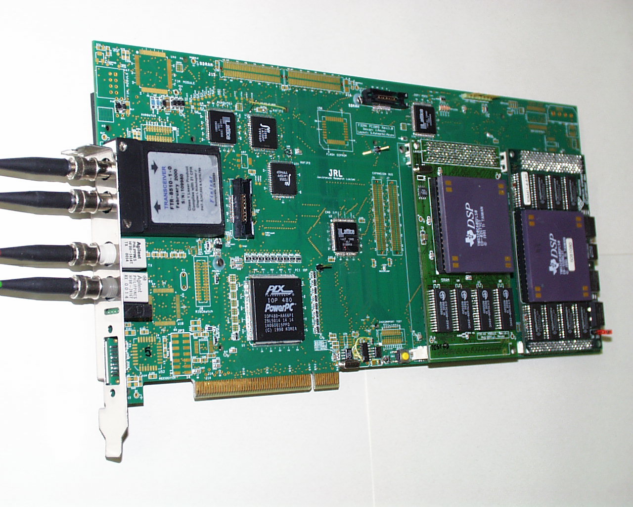
Figure 2a: FIERA SPARC including PCI board.
In general, the ultimate data rate limit of the FIERA system is established by the 50 million word limit of the fiber optic data link. However, it would be possible to pass up to 75 million pixels per second, if the data is 14 bits/pixel and 3 pixels are packed into every pair of 21 bit words. FIERA also has the option of passing data directly from the interface board to an external computer (usually a Real-Time Computer for AO applications); this link can run at the maximum 50 million words per second of the fiber optic link.
FIERA can also be triggered by the standard ESO Time Interface Module. This interface provides timing pulses with absolute accuracy of 10 microseconds, as derived from GPS satellite signals ([5], [6]). FIERA´s embedded computer was initially a VME bus SPARC but was upgraded to a SPARC with PCI bus.
Within the VLT control system, the embedded computer of FIERA is called a Sparc-based local control unit (SLCU).
3.2 Detector Head Electronics
The detector head electronics is a combination of five custom developed printed circuit boards: backplane, communication board, analog bias board, clock driver board and video signal processing board. These boards are 6U high (233 mm) and 220 mm deep.
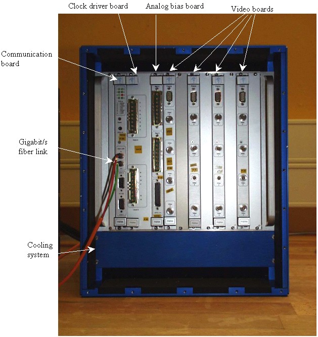
Detector Head Box
The 11 slot backplane uses VME standard P1 and P2 connectors but with ESO specific pin allocation. The 11 slot size was chosen as the maximum that could maintain the quality of 50 MHz command and data buses. This size is also adequate for all systems foreseen in the next few years at ESO, including those that utilize 16 readout ports (e.g. adaptive optics, wide field of view).
The communication board is the counterpart of the PCI interface board which resides in the embedded computer, incorporating a Finisar transceiver and Hewlett-Packard HDMP modules. The communication board transfers commands from the C40 DSP sequencer to the command bus on the backplane and takes data from the backplane’s data bus and sends it down the fiber link to the embedded computer.
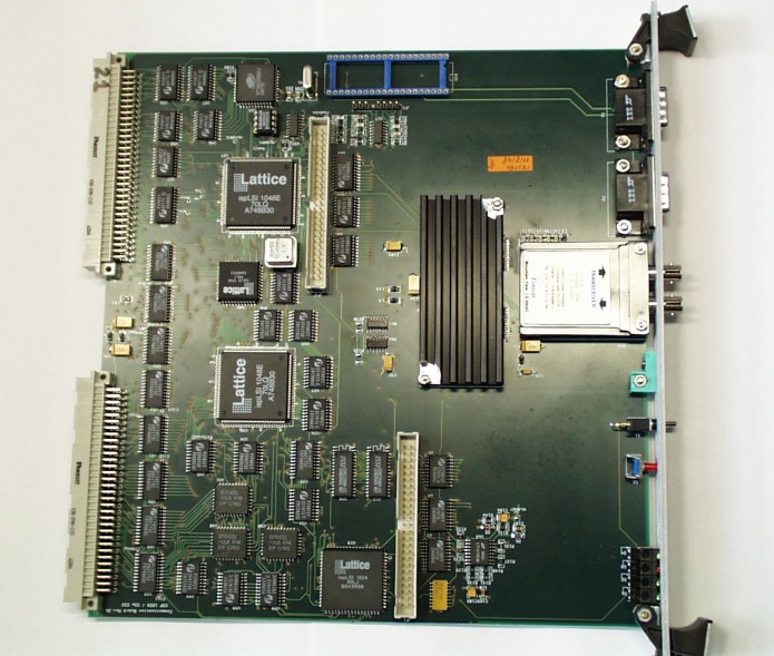
Communication Board
The analog bias board produces 32 bias levels that are fully programmable over a range of - 15 to + 30 V. There are hardwired protection switches that can be used to limit the output voltages of biases which could damage the CCD (e.g. output drain, output source and dump drain).
Bias Board
The clock driver board produces 14 clocks that can run at rates up to the 50 MHz. The clock driver board is actually a mini-motherboard with SIMM modules inserted to produce the clock voltages. We developed two types of SIMMs for FIERA:
- A fully programmable bi-level SIMM that can have the two output voltage levels remotely set to an accuracy of 0.1 V over the range - 14 V to + 14 V.
- A fully programmable multi-level SIMM that can output any voltage level between - 14 V and + 14 V, to an accuracy of 0.1 V (256 levels), with an update rate of 50 MHz.
Both of these clock driver designs can drive large currents 2A (only limited by the power supply capabilities); either for running CCDs very fast or for driving a large number of CCDs with a single clock driver board, as we planned for our 32-CCD 16k x 16k mosaic of OmegaCAM.
At the time FIERA was developed, the fully programmable and very fast multi-level SIMM was a new advance in clock drivers. The feature was implemented to maximize CTE, minimize spurious charge generation and possibly implement anti-blooming clocking in the best way possible.
Both the analog bias and clock driver boards have full telemetry built into design; all voltages can be measured. There are relays between the boards and the CCD so that all voltages can be verified before sending power to the CCD.
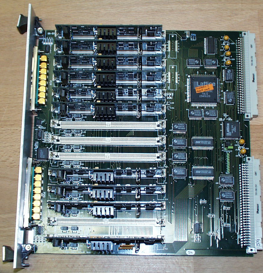
Clock board
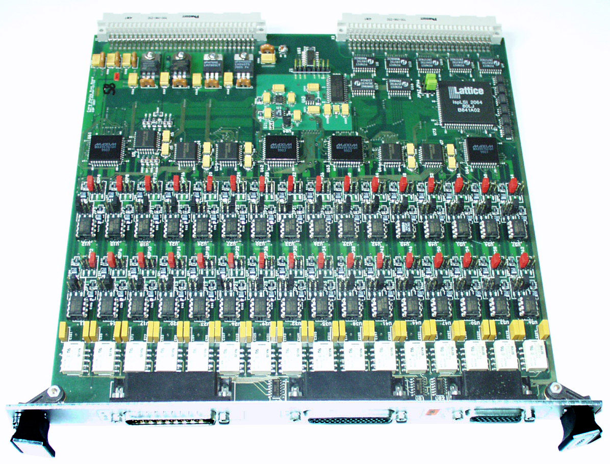
The video signal processing board includes amplifiers, correlated double sampling (CDS) and analog-to-digital conversion for four channels at rates to 2000 kps (2 million pixels per channel per sec) with 16 bits per pixel. The limit is set solely by the A/D converter. Initially, we did not foresee any advantage for speeds faster than 1000 kps and started only buying the less expensive 1 MHz A/D for most of ESO’s systems. The systems that run Tektronix or Loral CCDs were equipped with 500 kHz A/D converters.
For the first implementations of FIERA, we wanted a system that could run at rates to 1000 kps. Thus, we implemented the clamp-and-sample approach to CDS, rather than the supposedly lower noise dual-slope approach. The initial idea was to overcome the approx. square root of 2 disadvantage of clamp-and-sample by oversampling and digitally processing the signal, and, if we were not able to achieve the lowest noise at slow speeds with this video board, as is required for long exposure spectroscopy, we would design a new video board that implements dual-slope. However, experience showed us that CDS, when properly implemented, can achieve tremendously good noise levels and therefore we had no need neither design a new video board neither implement oversampling.
For CDS, there is a choice of four software selectable RC filter time constants placed just prior to the clamp circuitry. There is a synthetic video signal generator on the board, using the design of the multi-level clock driver, so that virtually any video signal can be generated.

4 Channels Video Board
The video board design and layout appear to be of good and solid quality. The rms noise of the board itself is 1.2 digital numbers and crosstalk is much less than 1 part in 100,000 when a highly saturated signal is put into one of the channels.
The FIERA detector head electronics is housed in an airtight box with fans and a heat exchanger with cooling liquid provided by an external source.
3.3 CCD Detector Head
All of ESO’s "dewars" are now made from a design that has two parts, a detector head and a cryostat that provides the cooling function. There are three different cryostat designs in use at ESO, two "bath" cryostats designs and a continuous flow cryostat that can provide cooling to a detector head for one month via an LN2 line from a 160 liter LN2 tank. The same detector head can be used with any of the cryostats (except for OmegaCAM which uses a custom-made cryostat due to its huge dimensions).
By using flex-rigid printed circuit boards for all of the CCDs inside the dewar we have been able to rapidly deploy a large number of CCD systems that are nearly identical.
Two different approaches are being used for the cryostat wiring. For Tektronix, SITe and Loral CCDs, a printed circuit board that is inside of the cryostat has been used to differentially amplify the video signal for transmission to the FIERA detector head electronics. The board inside the cryostat also provides passive filtering to the clock and bias lines. For EEV and MIT/LL CCDs, we developed a new set of printed circuit boards with the pre-amplifier circuitry placed in a small box outside of the cryostat, as shown in Fig. 1. There is passive filtering on clock and bias lines placed on the printed circuit boards inside the cryostat.
For the pre-amplifier inside the cryostat, there is a single hardwired gain. In the pre-amplifier box placed outside of the cryostat, there is a choice of two gains, software selectable from the embedded computer. Our approach was to maximize gain as much as possible at the front end, since in some instruments we must allow cable lengths of 1 to 2 meters between the pre-amplifier and the video signal processing board.
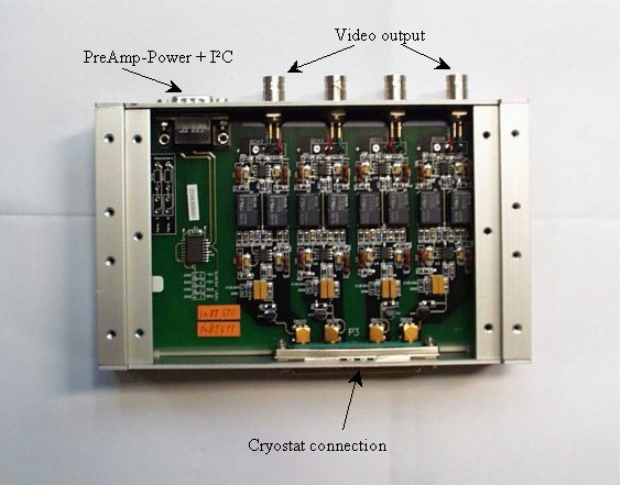
PREAMP BOX
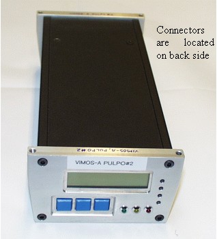
3.4 PULPO Housekeeping Box
The PULPO module is used to measure and control temperature (via heaters) and for measuring the vacuum of the cryostat. It also can run shutters and transmit and receive optically isolated signals from shutter drivers. PULPO communicates to FIERA via the RS-232 port on the SPARC. PULPO is described in detail in [7].
PULPO
PULPO has been upgraded to cope with more temperature sensors and heaters. The new PULPO, named PULPO-II is shown below. PULPO-II has internally a PC card-size running Linux (click here to see image).
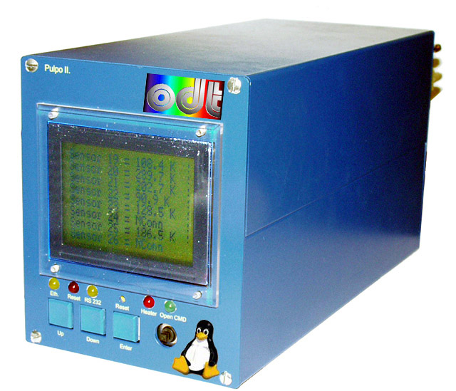

PULPO-II front and back
3.5 DC power supply module
As for any CCD controller, FIERA requires a number of DC voltages. Since size and weight were not significant constraints for ESO’s optical detector systems at the time the design of FIERA was undertaken, we decided to take a conservative approach for DC power generation. We use a switching power supply to generate the 24 V needed by PULPO and linear power supplies to generate the 5, ± 15 and 30 V needed by the FIERA detector head electronics.
The DC power supply module is housed in an airtight box with fans and a heat exchanger as done for the detector head electronics.
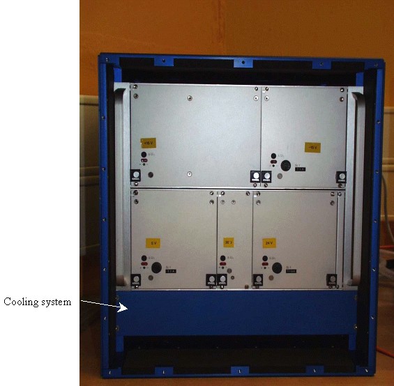
FIERA Power Supply box
4. Microsequencer
A significant feature of the FIERA design is the implementation of a microsequencer that provides local generation of control bits. This design minimizes the number of high speed signals that are distributed across the detector head electronics backplane and it provides a virtually unlimited number of high speed control bits. The microsequencer is the key to realization of the high speed multi-level clock drivers and the 256 level synthetic video signal generation.
The main sequencer in FIERA is the Texas Instruments C40 DSP that is on the interface board within the embedded computer. This C40 puts out relatively high level commands to the detector head, such as "perform a parallel line shift" or "read out 1000 pixels".
These commands are distributed simultaneously to all of the microsequencers that are located in the detector head. The communication, clock driver and video boards all contain microsequencers (no microsequencer is needed on the analog bias board). After receiving a command, the microsequencers output the bit patterns that correspond to the operation requested. For instance reading out a pixel involves proper timing of the following signals:
- clock driver board - serial phases 1-3, reset gate, summing well
- video board - clamp, sample, output data to data bus
- communications board - read in data, put data onto fiber link
The microsequencer consists of a state machine combined with a SRAM (static RAM) memory chip. The state machine works as complex counter cycling through address locations and clocking out data from the SRAM. The counter function of the microsequencer is performed by a programmable logic array, and it only needs 3 values to run a pattern (start address of pattern, length of the pattern and number of times to repeat a pattern).
For the microsequencer design to work properly, all microsequencers must work in lock step at all times, since there is no communication between microsequencers. Care had to be taken with the distribution of the commands and the microsequencer clock. The C40 DSP software keeps track of the length of the patterns "in the queue" and puts out the commands for successive patterns at exactly the correct clock transition. We have tested this operation thoroughly to be certain that successive clock patterns have seamless transitions. One attribute of the microsequencer that makes this task easier is that it has a pipeline at its input.
In order to save memory locations in the SRAM, the clock frequency can be divided to utilize the minimal number of memory locations for storage of each pattern. The microsequencer clock division is performed by loading a register on the communication board. Of course, the microsequencers must finish any previously commanded patterns prior to changing the clock speed.
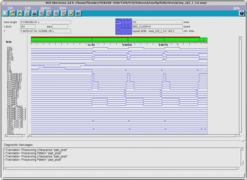
WES software, Editing and creating readout patterns
5. Control Software
The software architecture of FIERA is discussed at length in paper [8]. In short, nearly all of the control software of FIERA resides in the SPARC and is written in C and C++. There are a set of DSP routines programmed in the C40 DSP which require DSP knowledge, but these are also written in C, not assembly language code. There was however a need for a few specialized C40 functions that had to be coded in assembler for the situations that have very tight timing requirements (e.g. adaptive optics). When operating in the VLT environment, there is no monitor or keyboard attached to the FIERA SPARCstation and so all commands are sent to FIERA via the instrument network. In this implementation, the FIERA software extends to a module that resides in the instrument computer and the interface between FIERA and the instrument is located inside the instrument workstation.
The protocol between FIERA and instruments is that FIERA receives commands or queries from the instrument software and delivers replies or images (in FITS format) to the instrument workstation software. FIERA software uses the real-time display (RTD) module developed for the VLT; this software enables virtually instantaneous display and analysis of the image data.
When FIERA is operated in standalone mode, the interface to instruments essentially migrates down to the FIERA SPARCstation and we operate FIERA as a standalone "instrument". All of the software developed for FIERA is thus used for either standalone mode or in conjunction with a VLT instrument. Since the FIERA software has a well defined interface, non-VLT software can access FIERA through a network interface (i.e. sockets). This has allowed us to put FIERA easily into any telescope environment, important for using FIERA at the telescopes also of ESO’s La Silla Observatory.
An important software module that was developed for FIERA is the Waveform Editing Software (WES), which makes it relatively easy to graphically program the patterns of the microsequencers. In addition, WES is used to generate the sequences that are used by the C40 DSP code to schedule the transmission of microsequencer commands. The split between microsequencers and the main sequencer (C40) is transparent to the user, and it is easy to rapidly develop clock patterns.
6. Development, Production and Deployment Schedule
We demonstrated that the architecture of FIERA was sound and that the microsequencer approach to system control works as designed.
FIERA has been integrated with CCDs from several manufacturers, including: a Tektronix 2k x 2k, a Loral 2k x 2k, the EEV 2k x 4k, EEV CCD50 for AO and the MIT/LL 420 x 420 frame transfer and 2k x 4k devices. Also FIERA achieved to control the Wide Field Imager 9 CCD mosaic, and is going to be used for the VST-OmegaCAM project.
While we had achieved some respectable noise results on the EEV device (6 e- rms noise at 300 kps), there was some lingering concern at to whether FIERA would have some fundamental problem with achieving lower noise. That question was resolved when FIERA was used in September 1999 with the UVES instrument to achieve 1.9 e- rms noise at 50 kps with the EEV 2k x 4k device. Note that this result was achieved with clamp-and-sample CDS.
To date, FIERA has been made in more than 20 copies, running on about 20 instrument (La Silla and Paranal) without any failures during operation. These statistics show how reliable FIERA is.
Acknowledgements
Although the FIERA design was initiated by the three authors of this paper, its current realization and performance is the product of the hard work by all members of ESO’s Optical Detector Team and other ESO group, including Dietrich Baade, Andrea Balestra, Claudio Cumani, Sebastian Deiries, Robert Donaldson, Reinhold Dorn, Christoph Geimer, Ali Mohammadzadeh, Samuel Muñoz, Holger Pieper, Gustavo Rahmer, Roland Reiss, Javier Reyes and Jesper Thillerup in Garching with critique and help from the La Silla ODT members - Jaime Anguita, Nicolas Haddad, Andres Rivera and Peter Sinclaire. The La Silla team developed the PULPO housekeeping module. The first prototype design and fabrication of the video board and the clock driver boards were done by SciMeasure Analytical Systems, led by Charlie Bleau. Design of the backplane was done by Helga Kasten. Gerhard Fischer has been invaluable in his assistance with prototype fabrication and construction, as has Eddy Pomaroli for finding electronics parts and specifying fabrication techniques. Fernando Pedichini of Osservatorio Astronomico di Roma helped design the analog bias board and visited Garching several times to work with our team. Johann Zipperer of Texas Instruments helped design the C40-based computer interface board. A "tiger team" review which provided valuable midcourse critique in December 1995 was staffed by Preben Noerregaard and Jens Klougart of the U. Copenhagen.
7. References
[2] Yamashita, H., Y. Matsunaga, M. Iesaka, S. Manabe and N. Harada (1988), "A new high sensitivity photo-transistor for area image sensors", IEDM 88, IEEE, pp. 78-81.
[3] Beletic, J., R. gerdes and J. Zipperer, 1996 " A DSP-based solution to remote control of detector head electronics for scientific CCD systems.", DSP-96, Munich
[5] M. Ravensbergen, K. Wirenstrand, 1995, "Time Reference System of the VLT Telescope Control Systems", SPIE vol. 2479.
[6] W.R. Lange, M. Ravensberger, 1995, "Time Reference System of the ESO Very Large Telescope", Ninth European Frequency and Time Forum, Besançon.
[7] Haddad, N. and P. Sinclaire (1997), "PULPO: Temperature, vacuum, shutter, LN2 level, all in one box", ESO Workshop on Optical Detectors for Astronomy, J. Beletic and P. Amico (ed.), Kluwer, Dordrecht, pp. xx-xx of these proceedings.
[8] Cumani, C. and R. Donaldson (1997), "The architecture for two generations of ESO VLT CCD controllers", ESO Workshop on Optical Detectors for Astronomy, J. Beletic and P. Amico (ed.), Kluwer, Dordrecht, pp. xx-xx of these proceedings.