About IRACE
The electronic part of the data-acquisition system IRACE consists of four main groups
The IR detector connected to the electronics inside the cryostat (CRE) gets clocks and biases from the Detector front-end (DFE) and delivers the analogue detector data signals to DFE. The signals are then digitized and send to the detector back-end (DBE) over a fiberoptic link. Within the DBE is a interface to transfer the data to the DMA controller in the data-acquisition computer (DAQ).
Cryostat Electronics
The IR array detector is placed inside the vacuum vessel and cooled to cryogenic temperatures. An interface board connects clocks and biases after filtering and protection circuitry to the IR detector. Interface boards for near IR detectors hold in addition cryo differential data line drivers located as close as possible to the detector signal pins for maximum interference noise immunity. There are three terminals on the vessel to separate analogue detector signals, clocks and the biases.
Detector Front-End
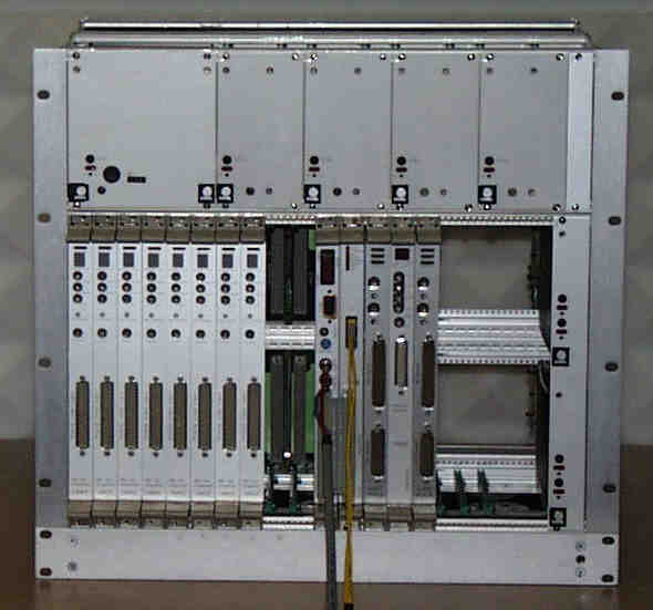
DFE consists of at least five boards, standard double Euro card size, placed in a VME size crate.
Sequencer as well as clock/bias driver and ADC modules can be cascaded, to adapt to individual system requirements.
- SEQUENCER
- CLDC (Clock/Bias driver)
- AQ (ADC’s and Preamplifier’s)
- GIGA (High Speed Data Link)
- TIF (Transputer Fiber optic Link Interface)
Detector Back-End
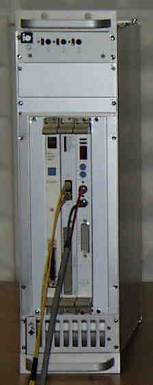
DBE consists of at least three modules in standard double Euro card size, placed in a VME size crate.
GIGA and TIF are the same modules type as on the front-end side
- TIF (Transputer Fiber optic Link Interface)
- GIGA (High Speed Data Link)
- DMA-Interface (Interface Gigalink Bus to NC DMA controller)
Data-acquisition computer
Commercial ULTRA SPARC computer(s) manufactured by SUN Microsystems.
Sequencer
Features
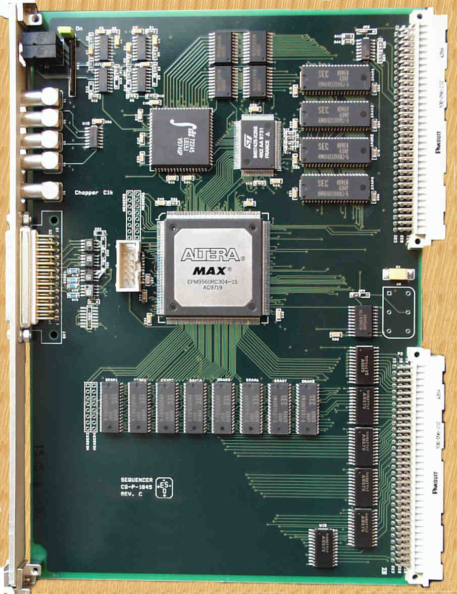
- Double Euro size module
- 48 digital clocks
- Time per word from 50 ns to 6350 ns
- Page organized patterns
- Page size 128 words of 48 Bits wide - 256 pages
- Page repeats from 1 to 63
- Quartz time base
General description
SEQUENCER is a page oriented clock pattern sequencer with a quartz time base of 50ns. The Sequencer system processor is a 32-bit transputer (T425) with 8 Mbytes DRAM. The words of a page are sequentially output, each word has an individual time count. Pages are held in a SRAM, 32K deep and 64Bits wide. Bit 0 to 6 determine the lifetime of the pattern and Bit 15, if set, states the end of a page. Bit 16 to 63 of a word are output as digital clocks, so there are 48 TTL clocks available. The maximum page length is 128 words. The time per word is between 50ns and 3.5 us, depending on Bit 0 to 6.
CLDC (Clock Driver and DC Bias)
Features
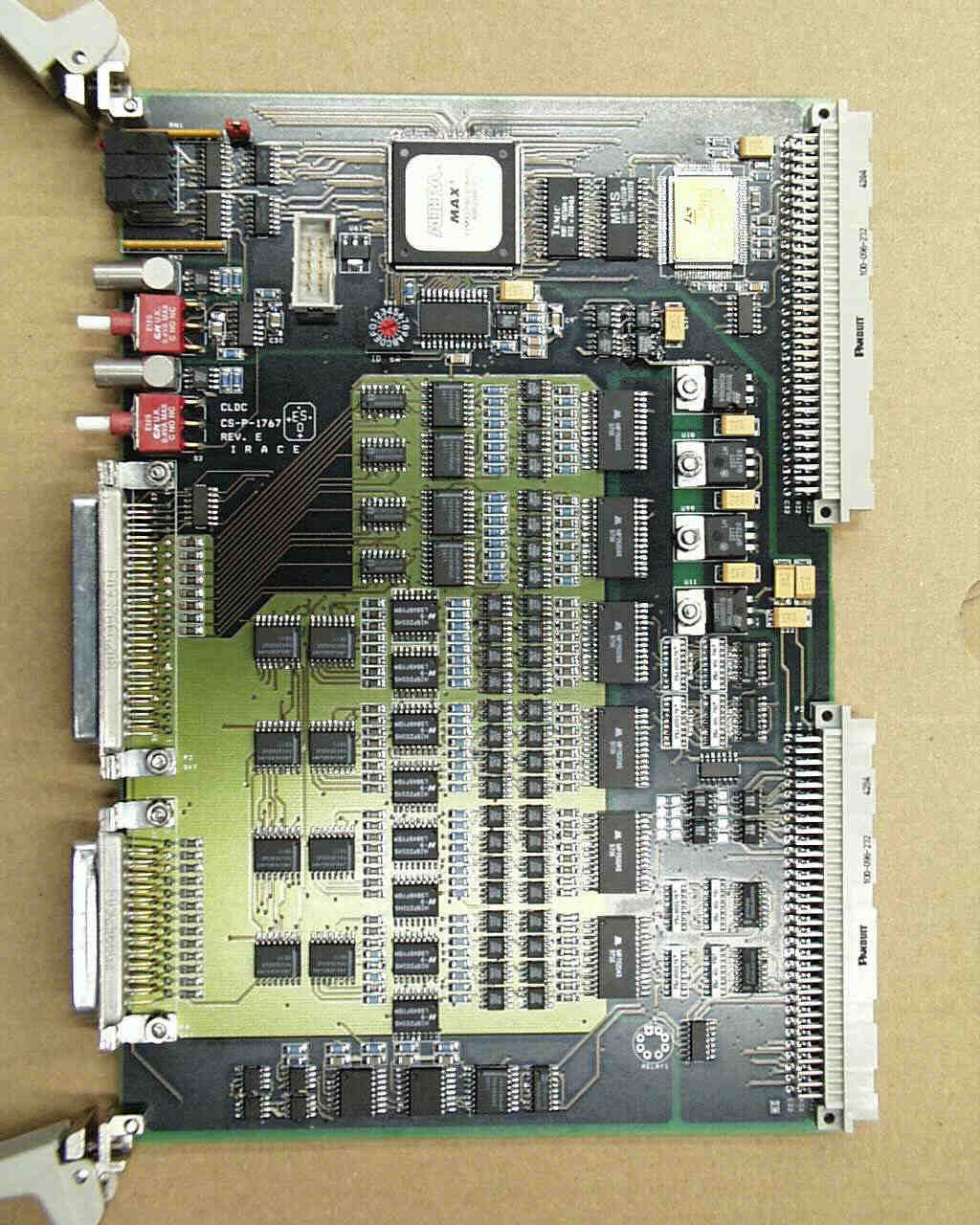
- Double Euro size module
- 16 low noise analog clocks out of 16 TTL signals
- 16 low noise bias voltages
- Telemetry of clock and bias voltages
- Temperature stable precise reference voltage
- Separately Digital analog connectors
- Temperature measurement of detector
- Monitoring of analog clocks
- Disable the output clocks through software and hardware
General description
This module works in cooperation with the SEQUENCER module, which generate the digital pattern for the detector readout. The incoming patterns from the SEQUENCER are TTL signals, that means only logical bit '1' or '0'. They are input control signal for the analog switch component, their every two output signals are connected together.
The Module provides 16 clock and 16 bias voltage generators with a maximum continuous output current drive of 80mA and an amplitude range of +/-10V. 12-bit DAC's and following operational amplifiers generate clocks bias voltages. Clocks and Bias voltages are output on the front connector. DSUB25 is for Clocks and DSUB37 is for Bias voltages foreseen. On board telemetry is done with a 12–bit ADC (3.3 m sec conversion time) connected to the input of the analog switches, via analog multiplexers. At power-up, the clock and bias outputs are disabled (10KOhm to GND). The outputs can be enabled through software and an external input signal. If the pin 36 of DSUB37 connectors goes low, the outputs of CLDC will be disabled. A voltage references circuit provides stable voltages for the DAC's. CLDC’s system processor is a T225 transputer.
AQ (Acquisition Module)
Features
- VME compatible
- Double Euro size module
- True differential analog inputs
- Low noise design
- Delay for ADC convert signal - software controlled up to 3 us by 50 ns steps
- AQ modules can be cascaded
- Monitor of ADC-inputs and the convert signal via front panel LEMO’s
- On board ADC-emulato
General description
Two different AQ modules are available:
- Four channel module with the fast ADCs (2000 ksps 16 bit)
- Sixteen channel module with the small ADC (333 ksps 16 bit )
Both of them have identical functioning, so that they can used in the same system without any changes. Only the number of channels and the convert time of ADCs are different.
Each acquisition module will be selected automatically as a master module by the slot-ID (if it is set). It then generates a header code, corresponding to the header, which is set in the status register one. Header word followed by the ADC data will put out over the GIGA bus. If the module is not a master, it just puts out the ADC data to the synchronous GIGA bus.
To be synchron to another AQ, there is a signal called "Moving bit". Each module sends his data if the "MovingBitIn" signal is low (low active), after them it generates for the next Aq module the signal "MovingBitOut" and so on...
AQ four channel
Features
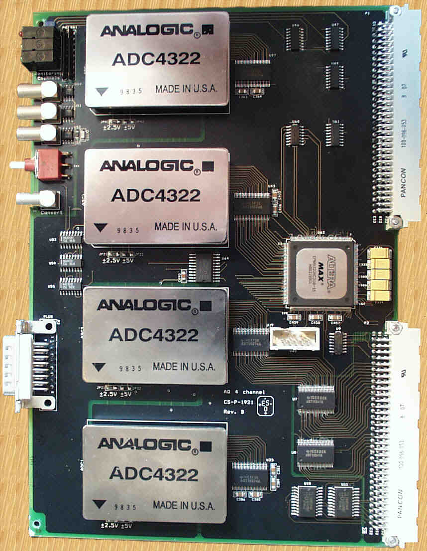
- Four 2 MHz ADC’s
- Two different input voltage ranges are scalable
- Four different signal filters - selectable by software
General Description
The acquisition module has four channels and contains minimum digital logic, so those low-level analog signals are not disturbed by digital noise. The differential analog input signals of each channel are input to a discrete buildup amplifier followed by a low pass filters in front of the ADCs. A conversion command triggers the ADCs. The data are immediately transferred to the output registers. The convert signal has a programmable delay from 750 nsec (offset value) to 3 sec in steps of 50 nsec.
AQ sixteen channel
Features
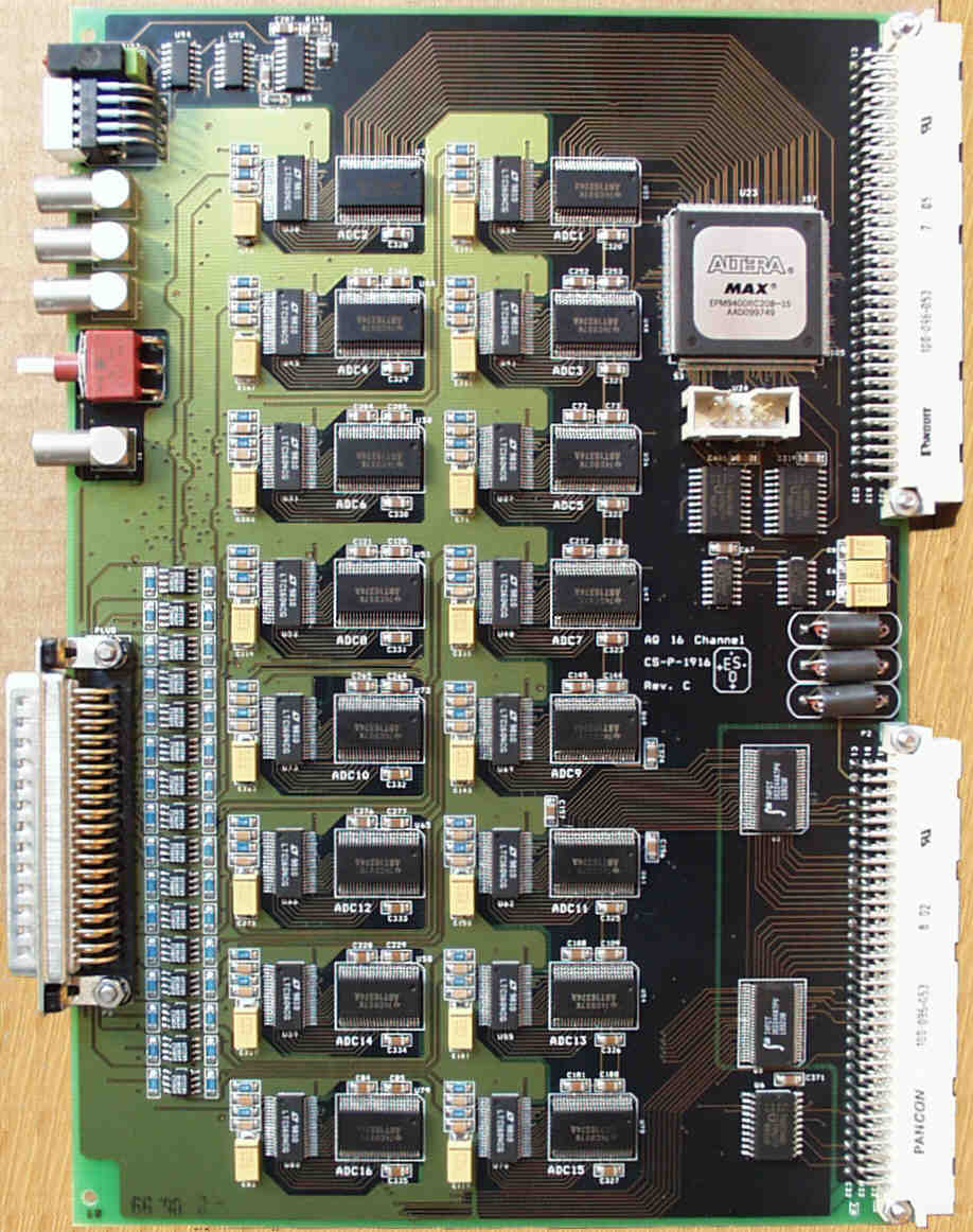
- Sixteen 3 us ADC’s
- Low noise design
General Description
The acquisition module has sixteen channels and contains minimum digital logic, so those low-level analog signals are not disturbed by digital noise. The differential analog input signals of each channel are input to a discrete buildup amplifier followed by a low pass filters in front of the ADCs. A conversion command triggers the ADCs, which has a convert time of 3 usec and the data are immediately transferred to the output registers. Each two output register (16 bit) send their data at the same time to the GIGA bus (32 bit width) on the P2 connector of backplane. The convert signal has a programmable delay from 0 to 3 sec in steps of 200 nsec.
GIGA (High Speed Data Link)
Features
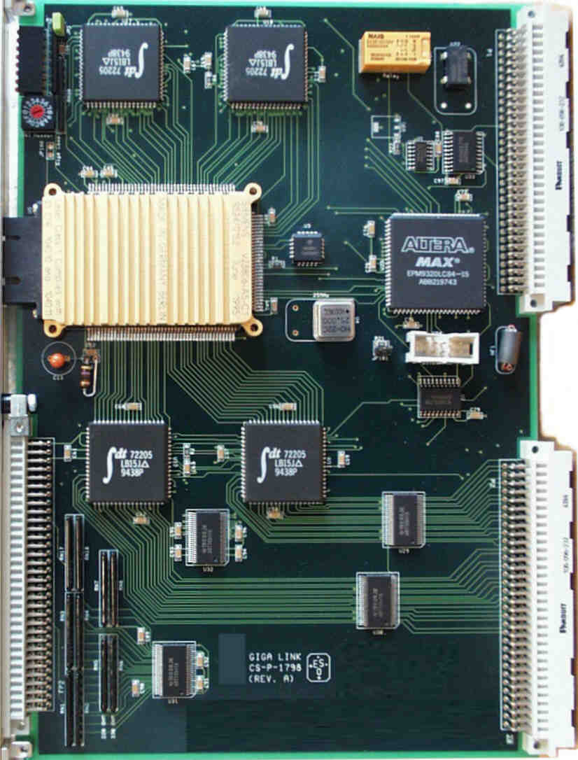
- Double Euro size module
- High speed fiber channel transmission of 1062.5 Mbaud (one gigabit / sec)
- Up to two kilometers fiber length possible
- 32 bit wide data input and output
- Data input and output FIFO buffered
General Description
GIGA is a VME 6HE module. It is a fiber optics transceiver with a transmission speed of one gigabit/s and uses for serial transmission a modified FIBERCHANNEL protocol. The data enter the module on the front panel connector from the synchronous Giga Bus to the fiber optics transmitter and the serial data from the fiber optics receiver leave the module to the synchronous Giga Bus on the VME P2 connector. The protocol and pin-out of the parallel bus is identical on transmitter and receiver side. Input and output data are FIFO buffered. The Transceiver hybrid itself (SIEMENS V23806) has a 32-bit wide data input and output and a 4-bit command input and output. The command signals are transmitted like data and are used to form the protocol of the parallel Giga Bus.
TIF (Transputer Fiber Link Interface)
Features
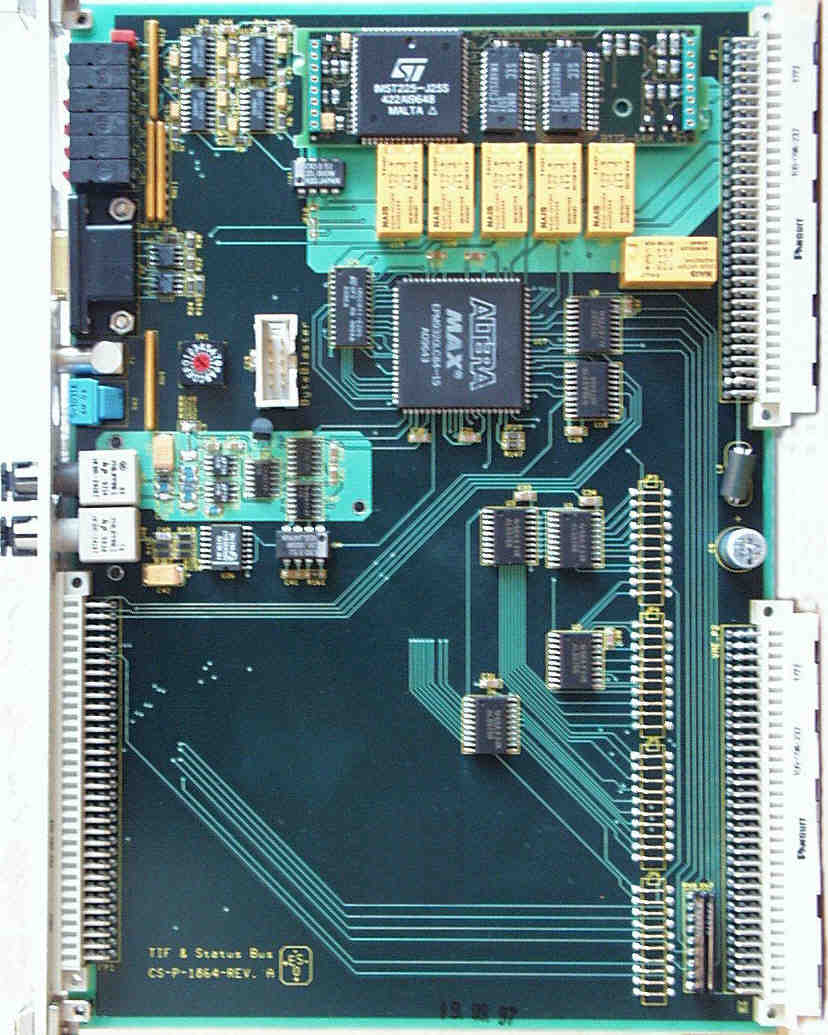
- Double Euro size module
- Fiber optic transputer link (Link in and Link out)
- LED monitor of Giga Bus data lines
- Control unit for status bus
General Description
TIF does primarily the conversion of the transputer link to a fiberoptic link between NC side and DFE and the distribution of transputer links in DFE. The TIF module is installed on the detector front end (DFE). It will convert the incoming fiber optic link to a Transputer link, route it to the transputer and de-multiplex the link signal into two other links. Over backplane the first is connected to the Sequencer link chain and the second to the clock driver (CLDC) link chain. If more than one sequencer is installed, the link is routed down through each sequencer. The same applies for the clock driver.
DMA-Interface (Interface of Gigalink Bus to ULTRA-SPARC DMA controller)
Features
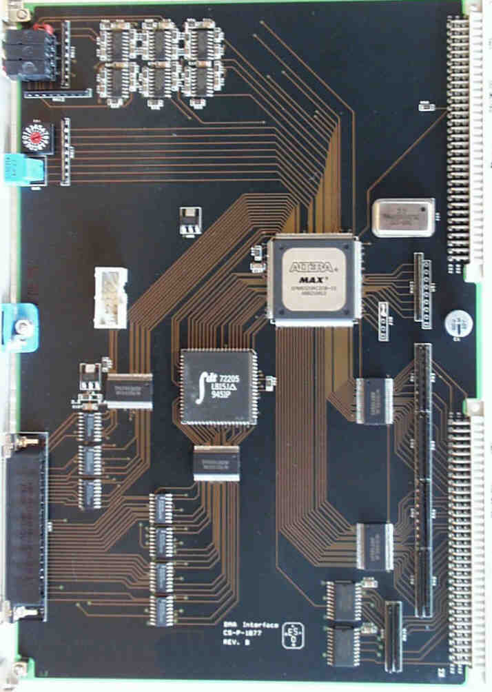
- Double Euro size module
- Interface to DMA controller SCD 60
- Data rate 60 MByte/s
General Description
DMA-IF interfaces the Giga Bus to the SUN Sbus DMA controller SCD 60. The 32Bit Giga Bus enters on P2 the DMA-IF. In an Altera PLD all logic for header recognition is done and the 32Bits of Giga Bus are de-multiplexed to the 16Bit size of the SUN Sbus DMA controller. From Altera, the data are feed into a FIFO. The FIFO output runs into a voltage level conversion circuit with the appropriate signals for SCD20 (TTL) or SCD60 (LVTTL). The appropriate driver circuits are installed at module assembly. The module than can only be used for either SCD20 or SCD60!.